How Computers Work Lecture 5 Memory Implementation
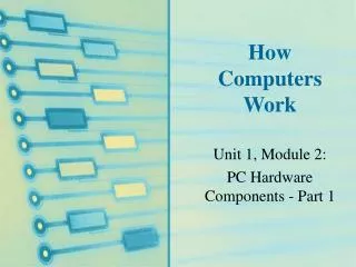
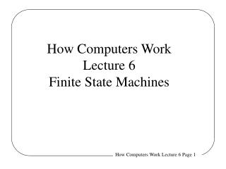
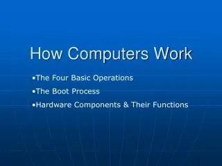
How Computers Work Lecture 5 Memory Implementation. PC Q. XADDR. RA1 Memory RD1. JMP(R31,XADDR,XP). ISEL. 0. 1. 31:26. 25:21. 20:5. 9:5. 4:0. OPCODE. RA. C. RB. RC. +1. 0. 1. OPCODE. Register File. RA1 RD1. Register File. RA2 RD2. SEXT. ASEL. BSEL. 0. 1.

How Computers Work Lecture 5 Memory Implementation
E N D
Presentation Transcript
PC Q XADDR RA1 Memory RD1 JMP(R31,XADDR,XP) ISEL 0 1 31:26 25:21 20:5 9:5 4:0 OPCODE RA C RB RC +1 0 1 OPCODE Register File RA1 RD1 Register File RA2 RD2 SEXT ASEL BSEL 0 1 2 1 0 A ALU B ALUFN A op B Z RA2 Memory RD2 PCSEL 0 1 0 1 2 WDSEL D PC WD Memory WA WD Register File WA RC WE WEMEM WE WERF A Top-Down View of the Beta Architecture With st(ra,C,rc) : Mem[C+<rc>] <- <ra>
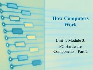
Today’s Lecture:How do we build these? RA1 Memory RD1 Register File RA1 RD1 Register File RA2 RD2 RA2 Memory RD2 WD Memory WA WD Register File WA WE WE
D Q E Recall the Enable-Controlled Register 32 32 CLK
D D D Q Q Q E E E How do we select 1 of 31 registers to read? . . .
D D D Q Q Q E E E A: Add an output selector. RD1 = <RA1> . . . 0 RA1
D D D Q Q Q E E E Q: How do we add a second port? RD1 = <RA1> . . . 0 RA1
D D D Q Q Q E E E A: Add a second multiplexor RD1 = <RA1> RD2 = <RA2> . . . 0 0 RA1 RA2
D D D Q Q Q E E E Q: How do we write selectively? RD1 = <RA1> RD2 = <RA2> . . . 0 0 RA1 RA2
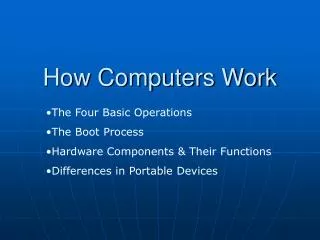
D D D Q Q Q E E E A: Use a decoder on the Enables WD 0 0 0 1 1 1 RD1 = <RA1> RD2 = <RA2> . . . WERF 30 30 30 31 0 31 0 31 RA1 RA2 WA
D D D D D D Q Q Q Q Q Q E E E E E E To minimize wires: WD WD 0 0 0 0 1 1 1 1 RD1 . . . . . . WERF RD2 30 30 30 30 31 31 0 31 0 31 RA1 WA RA2
D D D Q Q Q E E E Q: What about the clocks? WD 0 0 0 1 1 1 RD1 = <RA1> RD2 = <RA2> . . . WERF 30 30 30 31 0 31 0 31 RA1 RA2 WA
D D D Q Q Q E E E A: Connect them all together. WD 0 0 0 1 1 1 RD1 = <RA1> RD2 = <RA2> . . . WERF 30 30 30 31 0 31 0 31 RA1 RA2 WA Clock
Minimize per-bit circuitry . . . . . .
Minimizing per-bit circuitry . . . . . . Sense Amplifiers
Q: What can we use for a switch? A: The Field-Effect Transistor
How do we implement multiple ports? • 2 Read and 1 Write Ports • For now, LD and ST instructions are mutually exclusive. • 1 RD + 1 RD/WR port needed • LD and ST are don’t happen that often • Most of the time only 1RD port necessary • Easy answer : Do them sequentially • Need a way to “stall” machine waiting for Mem
Q: How do we stall this machine? PC Q XADDR RA1 Memory RD1 JMP(R31,XADDR,XP) ISEL 0 1 31:26 25:21 20:5 9:5 4:0 OPCODE RA C RB RC +1 0 1 OPCODE Register File RA1 RD1 Register File RA2 RD2 SEXT ASEL BSEL 0 1 2 1 0 A ALU B ALUFN A op B Z RA2 Memory RD2 PCSEL 0 1 0 1 2 WDSEL D PC WD Memory WA WD Register File WA RC WE WEMEM WE WERF
A: Stalls are done by: • Disabling WERF • Disabling Memory Write • Disabling PC write
Another Approach - Increasing Memory Bandwidth • Make memory twice as wide • 64 Bits Instead of 32 • Should work out in the long run, as 2 words are read per machine cycle, but • Words read are next to each other in address space • Need a place to stash the extra word • Sometimes, the stashed word isn’t used.
Summary • What Did we learn today? • How to Implement Registers + Big Memory • Multi-Port Big Memories aren’t easy • Sequential Access (stalls + extra logic) • Wide Access + Some sort of cache + extra logic • Recitation • Review of today’s lecture