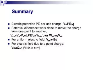
Summary
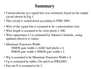
Summary. Current density in a signal line was estimated, based on the simple circuit shown in Fig.1. This circuit is scaled down according to ITRS 2003. Wire of the signal line is assumed to be a intermediate wire. Wire length is assumed to be (wire pitch) x 200.

Summary
E N D
Presentation Transcript
Summary • Current density in a signal line was estimated, based on the simple circuit shown in Fig.1. • This circuit is scaled down according to ITRS 2003. • Wire of the signal line is assumed to be a intermediate wire. • Wire length is assumed to be (wire pitch) x 200. • Wire capacitance Ci is estimated by Sakurai’s formula , using updated effective k values. • Minimum Transistor Width: NMOS gate width = (ASIC half pitch) x 4 PMOS gate width = NMOS gate width x 2 • Wg is assumed to be Minimum Transistor Width x 8 • Cg is estimated by tables 35a and b in ITRS2003. • Fan out N is assumed to be 3.
Average Imax = f *(Cg*Wg *N+Ci) *Vdd Average Imax (via) = Average Imax A Model for the Calculation - Tr width=Min Tr width x 8 Vdd Cg*Wg Imax Ci Intermediate wire(L=wire pitch x 200) Cg*Wg Fan out N=3
Calculation of Average Jmax (based on ITRS2003) Based on 2003 road map (Rev.1) Year 2003 2004 2005 2006 2007 2008 2009 2012 2015 2018 Technology node MPU/ASIC 1/2pitch 107 90 80 70 65 57 50 35 25 18 Width(nm) @Intermediate 160 137.5 120 107.5 97.5 87 78 55 39 27.5 Height(nm) @Intermediate 272 233.75 204 182.75 175.5 156.6 140.4 104.5 74.1 55 Vdd (V) 1.2 1.2 1.1 1.1 1.1 1 0.9 0.8 0.7 x 1 Gate Width (mm)* 1.284 1.08 0.96 0.84 0.78 0.684 0.6 0.42 0.3 0.216 x 8 Gate width = Wg (mm) 10.272 8.640 7.680 6.720 6.240 5.472 4.800 3.360 2.400 1.728 Physical gate length (mm)** 0.045 0.037 0.032 0.028 0.025 0.022 0.020 0.014 0.010 0.007 Inversion Gate Dielectric Value (nm)** 2.100 2.000 1.800 1.700 1.300 1.200 1.200 1.100 1.000 0.900 Parasitic Fringe/Overlap Cap (fF/mm) 0.240 0.240 0.240 0.230 0.220 0.200 0.190 0.150 0.120 0.080 Cg @ W=1mm(fF/mm) 0.979 0.878 0.853 0.798 0.883 0.833 0.765 0.589 0.465 0.348 Cg x Wg (fF) 10.059 7.588 6.554 5.364 5.513 4.555 3.672 1.979 1.116 0.602 Frequency (MHz)*** 3088 3990 5173 5631 6739 8330 9920 16735 25616 35020 Fan out : N 3.000 3.000 3.000 3.000 3.000 3.000 3.000 3.000 3.000 3.000 Wire capacitance (fF/mm) 0.205 0.199 0.199 0.198 0.174 0.174 0.174 0.151 0.120 0.110 Wire length :Pitch*200 (mm) 64.000 55.000 48.000 43.000 39.000 34.800 31.200 22.000 15.600 11.000 Total Wire Cap (fF) 13.109 10.939 9.547 8.509 6.790 6.059 5.432 3.321 1.864 1.212 Total Cap (fF) 43.287 33.704 29.208 24.602 23.328 19.725 16.448 9.259 5.212 3.017 Average Imax(nA) 160405 161373 166202 152385 172929 195671 275254 213460 146026 73967.9 Average Jmax (MA/cm^2) 0.369 0.502 0.679 0.776 1.011 1.436 2.513 3.714 5.053 4.890 * Minimum NMOS gate width= (ASIC half pitch)*4, Minimum PMOS gate width=NMOS gate width*2 ** from Table 35a and 35b **: from Table 4c( not updated)