Optimizing Interconnect Design: Addressing Crosstalk and Power Consumption Challenges
This comprehensive overview delves into the intricacies of interconnect design, focusing on crosstalk mitigation and power optimization techniques. It discusses modifying wire topology, resizing wires, and buffer insertion strategies, specifically for multipoint nets. The analysis touches on methodologies like the Van Ginneken algorithm for buffer placement and employs the Elmore model for delay calculations. Additionally, it emphasizes the significance of minimizing glitches to reduce power consumption and advocates for algorithmic solutions to analyze coupling effects and improve signal integrity in digital circuits.

Optimizing Interconnect Design: Addressing Crosstalk and Power Consumption Challenges
E N D
Presentation Transcript
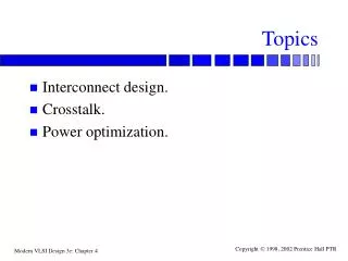
Topics • Interconnect design. • Crosstalk. • Power optimization.
Interconnect • Even assuming logic structure is fixed, we can: • change wire topology; • resize wires; • add buffers; • size transistors.
Multipoint nets • Two-point nets are easy to design. • Multipoint nets are harder: • How do we connect all the pins using two-point connections?
Spanning tree Steiner tree Steiner point Styles of wiring trees source sink 1 sink 2
Sized Steiner tree source Feeds both branches sink 1 Smaller currents in each branch sink 2
Buffer insertion in wiring trees • More complex than placing buffers along a transmission line: • complex topology; • unbalanced trees; • differing timing requirements at the leaves.
Van Ginneken algorithm • Given: • placements of sources and sinks; • routing of wiring tree. • Place buffers within tree to minimize the departure time at the source to meet all the sink arrival times: • Tsource = min i (T i -D i) • T i = arrival time at node i, D i = delay to node I.
Delay calculation • Use Elmore model to compute delay along path from source to sink.
Recursive delay calculation • Recursively compute Elmore delay through the tree. • Start at sinks, work back to source. • r, c are unit resistance/capacitance of wire. • Lk is total capacitive load of subtree rooted at node k.
Modifying the tree • Add a wire of length l at node k: • Tk’ = Tk - r/Lk - 0.5rcl. • Lk’ = Lk + cl. • Buffer node k: • Tk’ = Tk - Dbuf - Rbuf Lk. • Lk’ = Cbuf. • Join two subtrees m and n at node k: • Tk’ = (Tm , Tn). • Lk’ = Lm + Ln.
Crosstalk • Capacitive coupling introduces crosstalk. • Crosstalk slows down signals to static gates, can cause hard errors in storage nodes. • Crosstalk can be controlled by methodological and optimization techniques.
Coupling and crosstalk • Crosstalk current depends on capacitance, voltage ramp. ic w1 w2 t Cc
Crosstalk analysis • Assume worst-case voltage swings, signal slopes. • Measure coupling capacitance based on geometrical alignment/overlap. • Some nodes are particularly sensitive to crosstalk: • dynamic; • asynchronous.
Coupling situations bus[0] a x r bus[1] sig1 bus[2] better worse
Layer-to-layer coupling • Long parallel runs on adjacent layers are also bad. siga bus[0] SiO2
Methodological solutions • Add ground wires between signal wires: • coupling to VSS, a stable signal, dominates; • can use VSS to distribute power, so long as power line is relatively stable. • Extreme case—add ground plane. Costs an entire layer, may be overkill.
Ground wires VSS sig1 VSS sig2 VSS
Crosstalk and signal routing • Can route wires to minimize required adjacency regions. • Take advantage of natural holes in routing areas to decouple signals. • Minimizes need for ground signals.
Crosstalk routing example • Channel:
Assumptions • Take into account coupling only to wires in adjacent tracks. • Ignore coupling of vertical wires. • Assume that coupling/crosstalk is proportional to adjacency length.
Crosstalk analysis • Want to estimate delays induced by crosstalk. • Effect of coupling capacitance Cc depends on relative transitions. • Aggressor changes, victim does not: Cc. • Aggressor, victim move in opposite directions: 2Cc. • Aggressor, victim move in same direction: 0.
Crosstalk analysis, cont’d. • Coupling effects depend on relative switching time of nets. • Must use iterative algorithm to solve for coupling capacitances and delays.
Power optimization • Glitches cause unnecessary power consumption. • Logic network design helps control power consumption: • minimizing capacitance; • eliminating unnecessary glitches.
Glitching example • Gate network:
Glitching example behavior • NOR gate produces 0 output at beginning and end: • beginning: bottom input is 1; • end: NAND output is 1; • Difference in delay between application of primary inputs and generation of new NAND output causes glitch.
Adder chain glitching bad good
Explanation • Unbalanced chain has signals arriving at different times at each adder. • A glitch downstream propagates all the way upstream. • Balanced tree introduces multiple glitches simultaneously, reducing total glitch activity.
Signal probabilities • Glitching behavior can be characterized by signal probabilities. • Transition probabilities can be computed from signal probabilities if clock cycles are assumed to be independent. • Some primary inputs may have non-standard signal probabilities— control signal may be activated only occasionally.
Delay-independent probabilities • Compute output probabilities of primitive functions: • PNOT = 1 - Pin • POR = 1 - Pi) • PAND = Pi • Can compute output probabilities of reconvergent fanout-free networks by traversing tree.
Delay-dependent probabilities • More accurate estimation of glitching. Glitch accuracy depends on accuracy of delay model. • Can use simulation-style algorithms to propagate glitches. • Can use statistical models coupled with delay models.
Power estimation tools • Power estimator approximates power consumption from: • gate network; • primary input transition probabilities; • capacitive loading. • May be switch/logic simulation based or use statistical models.
Factorization for low power • Proper factorization reduces glitching. bad good
Factorization techniques • In example, a has high transition probability, b and c low probabilities. • Reduce number of logic levels through which high-probability signals must travel in order to reduce propagation of glitches.
Layout for low power • Place and route to minimize capacitance of nodes with high glitching activity. • Feed back wiring capacitance values to power analysis for better estimates.