Download
1 / 32
320 likes | 607 Views
Lens Aberration Aware Timing-Driven Placement. Andrew B. Kahng †‡* Chul-Hong Park ‡ Puneet Sharma ‡ Qinke Wang † CSE † and ECE ‡ Departments, UC San Diego *Blaze DFM, Inc., Sunnyvale, CA. Outline. Lens Aberration and Background Placement Formulation and Solver

E N D
Lens Aberration Aware Timing-Driven Placement Andrew B. Kahng†‡* Chul-Hong Park‡ Puneet Sharma‡ Qinke Wang† CSE† and ECE‡ Departments, UC San Diego *Blaze DFM, Inc., Sunnyvale, CA
Outline • Lens Aberration and Background • Placement Formulation and Solver • Aberration-Aware Timing Flow • Experiments • Summary
Lithography System Illumination Source • Lithography tool images a complex chip pattern with billions of pixels on wafer • Full-wafer exposure Step-and-repeat Step-and-scan system • Produce multiple copies of chips with one mask Lens Slit Lens Condenser Lens Mask Projection Lens Wafer
Image plane Illumination ray Lens Aberration • Lens Aberrations: image distortion induced by imperfect lens system • Optical path differences among light rays wavefront deviation from reference sphere at the exit pupil blur and distortion of images • Variety of effects on lithographic imaging shifts in image position, image asymmetry, reduction of process window
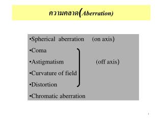
Spherical Astigmatism Coma Zernike Aberration Coefficients • Zernike Coefficients represent wavefront aberrations • 36 Zernike terms • Coma image asymmetry, pattern-dependent image shift • Astigmatism CD difference between horizontal, vertical lines • Spherical changes best DOF between dense/isolated patterns
Astigmatism X-coma Spherical Y-coma different Lens Position same Reticle (mask) map Zernike Coefficients with lens field • Slit scans from one side of the field to another • Zernike coefficients vary with position in the lens field CD also varies along horizontal direction CD stays constant along vertical direction • Astigmatism variation pushes designer toward single-directional layouts • Gate CDs of each master cell change according to lens position • Device performances vary across the chips in a lens field
An Example: Coma Aberration • Coma Aberration path difference in the horizontal direction CD asymmetry between left and right devices in pattern shown • CD variation: -15nm to 20nm in early 193nm scanners CD skews between devices increase circuit delay
Impact on Gate CD • Impact on average cell delay varies with location in lens field Average CD 93nm – 97nm for NAND2X4 • Different devices in a cell affected differently • CD skew: Max difference in CD of devices in a cell CD Skew up to 5nm for NAND2X4
Impact on Gate Delay • Impact on average cell delay varies with location in lens field NAND2X4 delay varies between -2% and 2% • Delay skew: Max difference over all timing arc delays NAND2X4 has delay skew increase of up to 60% • Input capacitance and slews increase with CD • Predictable “fast” and “slow” regions due to aberration • Place setup-critical cells in the fast regions, and place hold-critical cells in the slow regions
Outline • Lens Aberration and Background • Placement Formulation and Solver • Aberration-Aware Timing Flow • Experiments • Summary
Placer: APlace • Global Placement (NP-hard)as a Constrained Nonlinear Optimization Problem: We divide the placement area into uniform bins, and seek to minimize total half-perimeter wirelength (HPWL) under the constraint that total cell area in every bin is equalized. minHPWL (x,y) s.t.Dg (x,y) = D for each global bin g • Dg (x,y) : density function that corresponds to the total cell area in a given global bin “g” • D: average cell area over all global bins
Non-Linear Optimization • Apply smooth approximation of placement objectives: wirelength, density function, etc. • Quadratic Penalty method • Solve sequence of unconstrained minimization problems for sequence of µ 0 • Conjugate Gradient solver • Find unconstrained minimum of a high-dimensional function • Memory required is only linear in problem size adaptable to large-scale placement problems
High Quality and Extensibility • IBM ISPD'05 Placement Contest • Testcases directly derived from industrial ASIC designs, preserve physical structure of design • Large amounts of whitespace, fixed blocks and (peripheral or area) I/Os, up to 2.1 million components • APlace2.0 was contest winner • Strong Extensibility • Wirelength-Driven Mixed-Size Placement [ISPD04, ICCAD04, TCAD05, ISPD05, ICCAD05] • Timing Driven Placement [ICCAD04] • Power Aware Placement [DAC05] • Voltage Drop Aware Placement [ICCD05] • Aberration-Aware Placement [DATE06]
Aberr-Aware Placement Formulation • WWL is sum of timing-weighted net HPWL values • Wa is weight of the aberration-aware timing-driven objective • gtv(xv) is delay function for cell v’s model tv • If there are multiple (n>1) chips, gitv(xv) is delay function for ith chip • We consider the maximum delay of cell v over all copies improve performance of slowest chips (with pessimism) • Goal: Minimize total timing-weighted delays of timing-critical cells and total timing-weighted net wirelength
Weight Function • Assign timing weights to cells based on timing criticality and path sharing Cell on a timing critical path receives a heavy weight where • : timing-criticality exponent • µ: expected improvement of the longest (or shortest) delay • Ts = (1-µ)maxπ{delay(π)} for setup-critical path Th = (1+µ)minπ{delay(π)} for hold-critical path slacks(π) = Ts -delay(π): slack of a setup-critical path π slackh(π) = delay(π)-Th: slack of a hold-critical path π • Compute a weight for each timing-critical path • Obtain the timing weight of a cell by summing up the weights of timing critical paths
Smoothing of Delay Variations • Purpose of smoothing • Delay functions have accurate values only at discrete locations • Use linear interpolation to get cell delays at continuous positions in lens field can compute gradients • Smoothing factor β
Outline • Lens Aberration and Background • Placement Formulation and Solver • Aberration-Aware Timing Flow • Experiments • Summary
Standard Cell GDS SPICE Netlist Library Characterization SPICE Model Delay Extraction Standard Timing Analysis Flow • Problem: With aberration, two instances of the same master should have different timing models !
Aberration-Aware Timing Flow Delay LUTs Standard Cell GDS Transistor-level Timing Library (TTL) SRAF Generation OPC Library Characterization SPICE Model Lens Position Lithography Simulation SPICE Netlist Print Image GDS CD Measurement LVS CD Measurement • Two main steps • Construct litho models get simulated gate CDs of each instance • Generate timing library models of all masters for different locations
Delay LUTs Standard Cell GDS Transistor-level Timing Library (TTL) SRAF Generation OPC Library Characterization SPICE Model Lens Position Lithography Simulation SPICE Netlist Print Image GDS CD Measurement LVS Original GDSII GDSII with SRAF GDSII with OPC OPC GDSII Generation • SRAF: Sub-Resolution Assist Feature (or Scattering Bar) • Extremely narrow lines do not print on wafer • Enhance process window • OPC: Optical Proximity Correction • Layout modification to match photo-resist edges to layout edge limited ability to compensate for aberration-induced CD error
Zernike coefficients • 8 measured sampling position 19 coefficient sets with 1.5mm stepsize using linear interpolation • Lithography simulation • Post-OPC GDSII and aberration parameters lithography simulation at 19 different field locations with different lithography models • Use Calibre PrintImage to generate different contour images Delay LUTs Standard Cell GDS Transistor-level Timing Library (TTL) SRAF Generation 19 Different Field Positions OPC Library Characterization SPICE Model Lens Position Lithography Simulation Model-2 Model-3 Model-4 Model-5 Model-6 Model-1 SPICE Netlist Print Image GDS CD Measurement LVS • Measure CD of each MOS device at all positions in lens field Lithography Simulation
Standard Cell GDS SRAF Generation OPC Lens Position Lithography Simulation Print Image GDS Transistor-Level Timing Library • LVS mapping • GDSII does not have device names, while SPICE identifies devices by their names • Perform LVS to establish correspondence • Transistor-level timing library • Contain variants for each cell corresponding to different locations in the field • Capture aberration-induced CD skew as delay skew • A simplified look-up table is also created for analytical placement Delay LUTs Transistor-level Timing Library (TTL) Library Characterization SPICE Model SPICE Netlist CD Measurement LVS
Netlist Aberration- Aware Placement Delay LUTs TrialRoute Transistor-Level Timing Library Aberration- Aware STA • Wire length • Timing (MCT) • Run Time Aberration-Aware Placement Flow • Timing-driven placement flow • Send intermediate placement to TrialRoute perform a fast global and detailed routing • Change the type of each cell in the netlist with horizontal position of lens field • Use a commercial tool perform accurate aberration-aware STA with TTLs • Use Conjugate Gradient Solver • Total timing-weighted cell delays are minimized
Outline • Lens Aberration and Background • Placement Formulation and Solver • Aberration-Aware Timing Flow • Experiments • Summary
Design Utilization (%) Chip Size (mm) #Cells #Nets AES 60 0.50 17304 17465 JPEG 60 1.41 118321 125036 Experimental Setup • Mentor’s CalibreOPCpro and SBar • OPC and SRAF insertion • Cadence SOC Encounter and SignalStorm • Placement & Route • Library characterization • Synopsys Design Compilerand PrimeTime • Synthesis and static timing analysis (STA) • Benchmark Circuit • Artisan TSMC 90nm Library, RTL designs from OpenCores.org
Experimental Run • Two Placement Runs • AberrPl_WL • Perform with HPWL objective and no RC extraction before timing analysis • Compare with wirelength-driven APlace (APlace_WL) • AberrPl_TD • Perform with timing-driven wirelength objective and RC extraction before timing analysis • Compare with timing-driven APlace (APlace_TD) • Experimental Metrics • HPWL, Wirelength and Minimum Cycle Time (MCT)
Comparison of APlace with AberrPl • AberrPL_WL: MCT(↑4.7%), HPWL(↓3.0%) and WL(↓1.4%) for AES MCT(↑8.4%), HPWL(↓2.7%) and WL(↓2.4%) for JPEG • AberrPL_TD: MCT(↑9.8%), HPWL(↓1.5%) and WL(↓1.7%) for JPEG
AberrPL_WL AberrPL_TD Impact of Delay Ratio • MCT, HPWL, and routed wirelength impacts with delay ratio • Performed for circuit AES with a variety of delay ratios • AberrPl_WL: MCT improvement increases with delay ratio to 4.7% • AberrPl_TD: MCT reduction of 8.4% with 2.7% increase of HPWL and 2.4% increase of trial routed wirelength
Impact of Scaling • Effect of chip size on performance improvement • Circuit AES using AberrPl_WL with a variety of scaling factors • Performance improvement decreases with the number of copies • As the chip is small, the variation is too small to have benefit • Chip with large size will benefit more from AberrPl techniques
Outline • Lens Aberration and Background • Placement Formulation and Solver • Aberration-Aware Timing Flow • Experiments • Summary
Summary • We have proposed an accurate aberration-aware timing analysis flow and a novel aberration aware timing-driven placement technique • Maximum improvement of AberrPlace • Minimum clock cycle time:~5% • Wirelength increase: ~2% • Ongoing research • We plan to improve our approach so that the total value (i.e., “selling price”) of all chips is maximized • Aberration-aware OPC (AberrOPC) can correct CD variation of each gate will combine AberrPlace and AberrOPC to enhance CD accuracy, reduce delay impact