Download
1 / 18
180 likes | 225 Views
This research explores the device physics approach to develop power-efficient blue microcavity lasers and resonant-cavity light-emitting diodes (LEDs) in III-nitride-based materials. The study focuses on optimizing power conversion efficiency and increasing output power while reducing chip area. The integration of highly reflective mirrors and substrate removal methods are investigated for enhancing power efficiency in UV-LEDs.

E N D
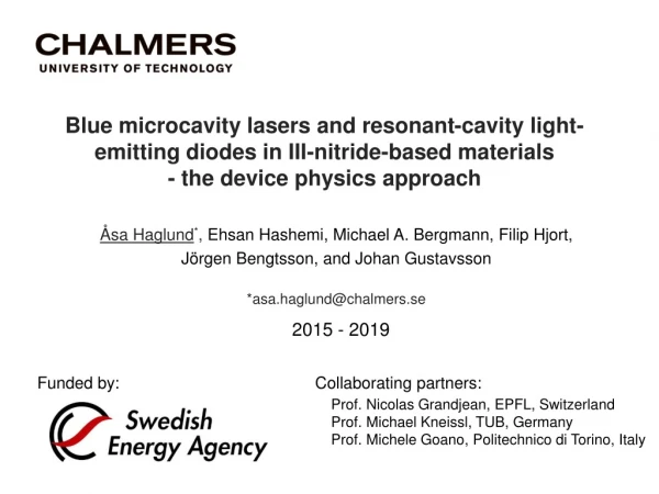
Blue microcavity lasers and resonant-cavity light-emitting diodes in III-nitride-based materials - the device physics approach Åsa Haglund*,Ehsan Hashemi, Michael A. Bergmann, Filip Hjort, Jörgen Bengtsson, and Johan Gustavsson *asa.haglund@chalmers.se 2015 - 2019 Funded by: Collaborating partners: Prof. Nicolas Grandjean, EPFL, Switzerland Prof. Michael Kneissl, TUB, Germany Prof. Michele Goano, Politechnico di Torino, Italy
Motivation: • Blue LEDs power efficient at ~10 A/cm2(droop) • Blue lasers power efficient at ~1000 A/cm2 • → Lasers = high output power / chip area with high power efficiency Chalmers University of Technology
Power-efficient microcavity lasers Optically guided waveguides Popt: 1 mW → 15.7 mWworld-record Power conversion efficiency = 8.9% 84% LEDs • Substrate removal method (AlGaN) to integrate highly reflective mirrors • ultra-smooth (Al)GaNsurfaces (<0.3 nm) • save 99% of the material • (reuse substrates) • boost power efficiency in UV-LEDs • today’s power efficiency < 10% E. Hashemi et al., Optics Express, vol. 25, no. 9, pp. 9556-9568, (2017) M. Kuramoto et al., APE, 11, 112101 (2018) M. Bergmann et al., IWN, OD14-7, (2018.) Åsa Haglund Chalmers University of Technology
Horizontal current and optical confinement p-GaN Current blocking layer (SiO2) Transparent current spreading layer (ITO) top propagating field Anti-guided Åsa Haglund Chalmers University of Technology 8/17
Horizontal current and optical confinement p-GaN Current blocking layer (SiO2) Transparent current spreading layer (ITO) Popt= 15.7 mW Popt= 1 mW WPE = 8.9% top propagating field Guided Anti-guided E. Hashemi et al., Optics Express, vol. 25, no. 9, pp. 9556-9568, (2017). M. Kuramoto et al., APE, 11, 112101 (2018) 8/17
High reflectivity mirror enabled by substrate removal • Smooth etched surfaces (RMS~0.3 nm) • First demonstration of AlGaN-etching by electrochemical etching uid Al0.06Ga0.94N / n-Al0.06Ga0.94N device layers airgap (n-GaN) Chalmers University of Technology
UVB LED Mesa diameter d = 80 µm
Introduction Applications of UVB light (280 – 315 nm) UVB EQE < 10 % Types of light sources Light-emitting diodes (LEDs) [1] https://www.ifkp.tu-berlin.de/fileadmin/i1/Kneissl/UV_LED_Efficiency_AUG_2017.pdf Chalmers University of Technology
LED designs Contributions to external quantum efficiency Improve light extraction efficiency through device design → Thin-film UVB LEDs Vertical thin-film flip-chip Thin-film flip-chip Chalmers University of Technology
Substrate removal Laser lift-off Alternative 2: Electrochemical etching [2] H. K. Cho et al., Semicond. Sci. Technol. 32, 12LT01 (5pp) (2017) [3] K. Kawasaki et al., Appl. Phys. Lett. 89, 261114 (2006) → Extend electrochemical etching towards AlGaN Chalmers University of Technology
Electrochemical etching of GaN Increased bend bending → hole concentration at semiconductor/electrolyte interface Bias voltage applied tothe semiconductor Increased hole density → anodic oxidation → dissolution of oxide in acid [4] Band-structure depends on the doping level uid-GaN Airgap (n-GaN) (n ≈ 5×1018 cm-3) [4] W.J. Tseng et al., J. Phys. Chem. 118, 29492 - 29498 (2014) Chalmers University of Technology
Electrochemical etching of AlGaN Sample design Setup Result uid-AlGaNmembrane AlGaN-layer with Al ≤ 50% can be removed completely Removed sacrificial layer Chalmers University of Technology
UVB LED fabrication process (1) Growth of UVB LED heterostructure by MOVPE [5] • n-doped etch stop layer with reduced doping → allows for electrical contacts [5] Enslin et al. J. Cryst. Growth 464, 185 (2017) Chalmers University of Technology
UVB LED fabrication process (2) Double mesa definition Contacts and Isolation Chalmers University of Technology
UVB LED fabrication process (3) Bonding, transfer and n-contact Removal of sacrificial layer • Electrochemical etching • 25 V vs. Ag/AgCl ref. • 0.3 M nitric acid Al/Ti/Au n-contact Au-Au thermocompression to Si carrier Chalmers University of Technology
UVB LED fabrication process (4) Processed LED Chalmers University of Technology
Summary IVP characteristics Optical spectrum RT j = 0.8 A/cm2 Mesa diameter d = 80 µm Chalmers University of Technology