Download

1 / 55
550 likes | 681 Views
Combinational Circuits and Sorting Networks. References. Selim Akl, Parallel Computation: Models and Methods, Prentice Hall, 1997, Updated online version available through website, Chapters 1-3, but primarily Chapters 2-3.

E N D
Combinational Circuits and Sorting Networks
References • Selim Akl, Parallel Computation: Models and Methods, Prentice Hall, 1997, Updated online version available through website, Chapters 1-3, but primarily Chapters 2-3. • Selim Akl, The Design of Efficient Parallel Algorithms, Chapter 2 in “Handbook on Parallel and Distributed Processing” edited by J. Blazewicz, K. Ecker, B. Plateau, and D. Trystram, Springer Verlag, 2000. • Henri Casanova, Arnaud Legrand, and Yves Robert, Parallel Algorithms, CRC Press, 2009, primarily Chapter 2.
Outline • To be added
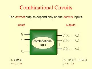
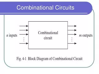
Combinational Circuits • A combinational circuit consists of a number of interconnected components arranged in columns called stages. • Each component is a simple processor with a constant fan-in and fan-out • Fan-in: Number of input lines carrying data from outside world or from a previous stage. • Fan-out: Number of output lines carrying data to the outside world or to the next stage.
Combinational Circuits (cont) • Component characteristics: • Only active after input arrives • Computes a value to be output in O(1) time, usually using only simple arithmetic or logic operations. • Component is hardwired to execute its computation. • Component Circuit Characteristics • Has no program • Has no feedback • Depth: The number of stages in a circuit • Gives worst case running time for problem • Width: Maximal number of components per stage. • Size: The total number of components • Note: size ≤ depth width
Two-way Combinational Circuits • Sometimes used as a two-way devices • Input and output switch roles • data travels from left-to-right at one time and from right-to-left at a later time. • Useful particularly for communications devices. • Needed to support the MAU (memory access unit) for RAM and PRAM
Batcher’s Odd-Even Merging Circuit • Diagram on previous slide shows Batcher’s odd-even merging circuit • Has 8 inputs and 9 circuits. • Its depth is 3 and width is 4. • Merges two sorted list of input values of length 4 to produce one sorted list of length 8. • Diagram is Figure 2.25 in Akl’s online text.
Recursive Design of Odd-Even Merge • A circuit for merging two sorted sequences of length m is called an (m,m) odd-even circuit. • An (m,m) odd-even circuit consists of two (m/2,m/2) odd-even circuits followed by a column of m-1 comparators • The (m/2,m/2) odd-even circuits are obtained by the same recurrence relationship
General Odd-Even Merging Circuit A circuit for merging two sorted sequences (x1, x2, …, xm-1) and (x1, x2, …, xm-1) is obtained as follows: • The odd-indexed elements of the two seqences (x1, x3, …, xm-1) and (y1, y3, …, ym-1) are merged to obtain a sorted sequence (u1, u2, …, um) • The even-indexed elements of the two seqences (x2, x4, …, xm) and (y2, y4, …, ym) are merged simultaneously to obtain a sorted sequence (v1, v2, …, vm) • Finally, the output sequence (z1, z2, …, z2m) is found by z1 = u1 z2m = vm z2i = min{ui+1, vi} z2i+1 = max{ui+1, vi} for i = 1,2, … , m-1
Correctness of (m,m) Merging Circuit • The (1,1) and (2,2) merging circuits are correct. • The first and last elements of general case are correct • z1 = u1 = min{u1, v1} is correct • zm = vm = max{um, vm} is correct • The correctness of algorithm depends on whether the following is true: • z2i = min{ui+1, vi} • Z2i+1 = max{ui+1, vi} • ui+1 is either a xj or a yj for an odd j. • If it is a xj, then all xk with k<j are above ui+1 and all xk with k>j must go below ui+1 • A similar statement holds if ui+1 is a yj for an odd j
Correctness of (m,m) Merging Circuit (cont) • Claim z2i = min{ui+1, vi} max{ui+1, vi} = z2i+1 min{ui+2, vi+1} = z2(i+1) = z2i+2 • Consider the case of i=1 first. Try to give an argument that z2 and z3 are correctly defined. • Remember that the sequence of u values consists of the x and y values with odd indices and these x & y values were already sorted. This is also true for the v-values. As a result, u2 and v1 have their location severely limited by their earlier position between x & y values. • This appears to be correct, looking at Fig 3.3 • Correctness is fully proved in Akl and in Casanova, et.al. by two different proofs. • This sort is correct.
Analysis of Odd-Even Merge • Width: The circuit takes 2minputs and produces 2m outputs. Each comparator handles two inputs, so its width is m • Depth: Let d(k) denote the depth of a circuit with k inputs • d(2) = 1 since this requires one comparator • d(2m) = d(m) +1 for m>1 (by Fig 3.3) • Solution to recurrence relation is d(2m) = 1+ log(m) • Note that d(2i) = d(2*2i-1) = 1+ log(2i-1) = 2i
Analysis of Odd-Even Merge (cont.) • Size: Let p(2m) be the number of comparators in the circuit. • p(2) = 1 • P(2m) = 2p(m) + (m-1) for m>1 (by Akl Fig. 3.3) • Solution to recurrence relation is p(2m) = 1+m log m • p(2i) = p(2*2i-1) = 1+ 2i-1 (i-1) • Running Time: Is the circuit’s depth, O(log m) • Very fast, as RAM takes O(m) • Number of comparisons: O(m log m) • Not optimal, as RAM requires O(m)
Batcher’s Odd-Even Sorting Circuit • Notation: Akl uses (m,m) and Casanova, et.al. use mergemto denote an odd-even merging circuit to merge two sorted sequences, each length m. • In the first phase, n/2 comparators, stacked vertically, are used to obtain n/2 sorted pairs of elements. • In next phase, n/4 merging circuits of size (2,2) are used to obtain n/4 sorted sequences of length 4. • In the final phase, 2 merging circuits of size (n/2,n/2) are used to obtain a sorted list of n • Output is the resulting sorted sequence of the input values
Analysis of Merge Sort • Width • The input and output is of size n and each comparator has two outputs, so the circuit width is n/2 • Depth • Let d(2i) be depth of a (2i-1,2i-1 ) odd-even merge sort. • We established earlier that d(2i) = i. • Then the length of an odd-even sort is
Merge Sort Analysis (cont 2/2) • Size • Let p(2i) denote the nr of comparators used by a (2i-1,2i-1 ) odd-even merge sort. • Earlier we established that p(2i) = 1+2i-1(i -1). • Since the ith phase uses n/2i such merging circuits, the total nr of comparators are
An Optimal Sorting Circuit • A complete binary tree with n leaves. • Note: 1+ lg n levels and 2n-1 nodes • Non-leaf nodes are circuits (of comparators). • Each non-leaf node receives a set of m numbers • Splits into m/2 smaller numbers sent to upper child circuit & remaining m/2 sent to the lower child circuit. • Sorting Circuit Characteristics • Overall depth is O(lg n) and width is O(n). • Overall size is O(n lg n).
An Optimal Sorting Circuit (cont) • Sorting Circuit is asymptotically optimal: • None of O(n lg n) comparators used twice. • (n lg n) comparisons are required for sorting in the worst case. • In practice, slower than the odd-even-merge sorting circuit. • The O(n lg n) size hides a very large constant of size approximately 6000. • Depth is around 6,000 lg n • This sorting circuit is a very complex circuit. • More details in Section 3.5 of Akl’s online text. OPEN QUESTION: Find an optimal sorting circuit that is practical, or show one does not exist.
A Memory Access Unit for RAM • A MAU for RAM is given by using a combinational circuit. • See Chapter 2 of online text or book-chapter. • Implemented as a binary tree. • The PE is connected to the root of this tree and each leaf is connected to a memory location. • If there are M memory locations for the PE then • The access time (i.e., depth) is (lg M). • Circuit Width is (M) • Tree has 2M-1 = (M) switches • Size is (M). • Assume tree links support 2-way communication • Using pipelining, this allows two or more data to travel the same or opposite directions at the same time.
Optimality of Preceding RAM MAU • The MAU will be implemented as a combinational circuit, so components must have a constant fan-out d. • A Lower bound on circuit depth for a MAU. • M memory locations M output lines (M) lower bound on circuit width. • At most ds-1 locations can be reached in s stages • In order for ds-1 M to be true, we must have s-1 = logd(ds-1 ) logd (M) • It follows that a lower bound on the MAU circuit depth for RAM is) (logd (M)) • Since (logd (M)) = (lg M), the preceding binary RAM MAU has optimal depth
A Comment on Optimality Proof • No advantage is gained by allowing a non-constant fan-out • Basically the same argument applies using d = maximum fan-out.
A Binary Tree MAU Implementation • Implemented as a binary tree of switches, as in Fig 2.28. • Processor sends a location “a” to access memory location Ua. • MAU decodes the address bit-by-bit. • For 1 i lg M, the switch at stage i examines the ith most significant bit. • If 0, the switch sends “a” to top subtree; otherwise “a” is sent to bottom subtree. • This creates a path from processor toUa. • If a value is to be written to Ua , this is handled by the leaf. • If a processor wishes to read Ua, the leaf sends this value back to processor along same path.
RAM MAU Analysis Summary • Depth and running time is (lg M). • Width is (M) • Tree has 2M-1 = (M) switches • Size is (M).
A MAU for PRAM • A memory access unit for PRAM is also given by Akl • Overview of how this MAU works discussed here • The MAU creates a path from each PE to each memory location and handles all of the following: ER, EW, CR, CW. • Handles all CW versions discussed (e.g., “combining”). • Assume n PEs and M global memory locations. • We will assume that M is a constant multiple of n. • Then M = (n). • A diagram for this MAU is given in Akl, Fig 2.30
Lower Bounds For PRAM MAU • Since there are M memory locations, M output lines are required and (M) is a lower bound on the circuit width. • By the same argument used for RAM, (lg M) is a lower bound on the circuit depth. • A Lower Bound on circuit size for an arbitrary MAU for PRAM. • Let x be the number of switches used. • Let b be the maximum number of states (i.e., configurations) possible for these switches. • E.g., binary switches can direct data 2 ways. • The entire circuit can have bx states. • Assume simplest memory access of EREW • With EREW, there are M! ways for M PEs to access M memory locations (a worst case)
Lower Bounds For PRAM MAU (cont) • Since the number of possible states for this circuit is bx, it follows that bx M! • Since lg(M!) = (M lg M) by corollary to Sterling’s Formula (pg 35 of CLR reference), x is (M logb M). • This shows circuit size is (M lg M). • The preceding lower bound must hold for the weakest access (i.e., EREW), so it must hold for all the other accesses as well.
PRAM MAU Memory Access Steps • Diagram in Akl’s Figure 2.30 is assumed below. • Assume that the ith PE produces the record (Instruction, ai, di, i) where “Instruction” is ER, CR, EW, etc. and aiis the memory address diis storage for read/write datum. • Each memory cell Uj produces a record (Instruction, j, hj) where “Instruction” is initially empty. j is the address of Uj hj is the memory content of Uj .
PRAM MAU Memory Access Steps • The sorting circuit in diagram sorts processor records using the memory address ai. • Ties broken by sorting on value of i. • The values of j in second coordinate of memory records are already sorted. • The two sorted sets are merged and sorted on their 2nd coordinate. • Two sets were already presorted on 2nd coordinate • In case of a tie, the processor record precedesthe memory record. • Comparators here are slightly more complex. • Must handle information transfers • Must handle arithmetic & logic operations
Memory Access Steps (cont) • Additionally, comparators must have bit to store straight/reverse routing information for use in reverse routing. • All necessary information transfers between processor records and memory records occur at within comparators in the merging circuit. • Possible since each processor record with memory address j is brought together in a comparator with the memory record with memory address j. • Information transfers include • Instruction field transfer to memory record. • For ER, the memory value is transferred to processor record (i.e., dihj) when these two records meet in a comparator. • For EWs, value to be written is transferred to memory record (i.e., hj di) when these two records meet in a comparator.
CR Memory Access • The transfers for a CR is more complex. • Recall each memory record enter on top half of the input to merge, but after merge it will immediately follow all PE records seeking to read its value. • When a memory record meets a PE record seeking its value, the memory value is transferred to a processor record (i.e., di hj) • Since memory input is at top of merge but will move past all PE records seeking to read it, the record for each Pj seeking to read Ui will meet the Ui record in a comparator
CW Memory Access • The CW action (e.g., common, priority, AND, OR, SUM) is also more complex. • Below description given for SUM. Others are similar. • After the processor and memory records are merged, the records of all processors wishing to write to the same memory location Uj are contiguous and precede the record for Uj . • During the forward routing, the Uj record will have met a PE wishing to write to it, and will have its instruction value set (e.g., CW-ADD) an its hj value set to zero.
CW Memory Access Steps (cont) • During reverse routing, each of these PE records and the Uj record trace out a binary tree that has memory location Uj as its root. • It is important to observe that Uj meets each Pk that wishes to write to Ujonce and only onceon both incoming and reverse routing. • When the record for a processor Pk writing to location i meets the record for Ui, the value recorded for Ui (initially set to 0) becomes di+hk . • The other Concurrent Writes are calculated similarly • Will need an extra memory component in Ui in case of PRIORITY Write to keep up with largest value.
Comparator size • Each needs to remember the line each record arrived on initially to use for reverse routing. • This allows memory records to be shipped back for a WRITE and processor records to be shipped back for a READ. • A one bit per record in each comparator is sufficient for reverse routing. • In case pipelining is used, comparators will need O(lg M) bits [since O(lg M) stages]. • Reasonable to provide O(lg M) bits for this, as registers are needed to handle values and addresses needed with a memory of size M.
Complexity Evaluation for Practical MAU • Assume that MAU uses the odd-even merging and sorting circuits of Batcher • See Figs 2.25 and 2.26 (or examples 2.8 and 2.9) of Akl’s online textbook • We assumed that M is (n). • Since the sorting circuit has the larger complexity • MAU has width O(M) = O(n) • MAU has running time O(lg2M) = O(lg2n) • MAU has size O(M lg2M) = O(n lg2n)
A Theoretically Optimal MAU • Next, assume that the sorting circuit used in MAU is the optimal sorting circuit • Since we assume n is (M), • MAU has width (M) = (n) • MAU has depth or running time (lg M) = (n) • MAU has size (M lg M) = (n lg n) • These bounds match the previous lower bounds (up to a constant) and hence are optimal.
Additional Comments • Both implementations of this MAU can support all of the PRAM models using only the same resources that are required to support the weakest EREW PRAM model. • The first implementation using Batcher’s sort is practical while the second is not but is optimal. • Note that EREW could be supported by the use of a MAU consisting of a binary tree for each PE that joins it to each memory location. • Not practical, since n binary trees are required and each memory location must be connected to each of the n binary trees.
0-1 Principle Proposition: A network R is a sorting network for arbitrary sequences if and only if it is a sorting network if and only if it is a sorting network for 0-1 sequences. • If R sorts arbitrary sequences, it obviously sorts 0-1 sequences. • We show that if R does not sort arbitrary sequences correctly, then R does not sort 0-1 sequences correctly. • Then WLOG, there exists a sequence x = (x1,x2, … , xn) and a position k such that R(x)k > R(x)k+1 • Note if f is an increasing sequence, a comparator has the same behavior on (y1,y2) as on (f(y1),f(y2)).
0-1 Principle (cont) • We define an increasing function f: {x1,x2, … , xn} {0,1} as follows: 0 if y < R(x)k f(y) = 1 if y R(x)k • Claim: R does not correctly sort the 0-1 sequence { f(x1), f(x1), …, f(x1)} • f ( R(x)k ) = 1 is output at position k • f ( R(x)k+1 ) = 0 is output at position k+1 • This completes the proof.
Proposition: The odd-even transposition sort is a sorting network. Proof: See initial part of Ch 8 slides (i.e., Mesh Model) in PDA-07 for a more complete proof. • We use the 0-1 principle to prove • Let (a1, a2, … , an) be a 0-1 sequence • Let k be the number of 1’s in sequence • Let j0 be the position of the rightmost 1. • Note a “1” only moves when it is on the right and a 0 is on left in a comparator • The 1’s never move to the left • The key is to follow movement of leftmost 1 and the rightmost 1. • Let j0 be position of right-most 1.