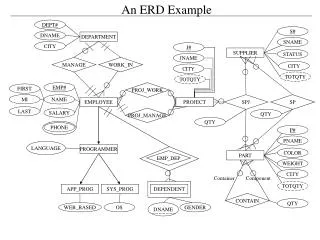
An example Program
An example Program. switch reading , the most basic computer input operation. Keyboards. A computer keyboard typically uses a microprocessor to scan the switches. Similarly in remote control units for TVs etc. row select lines. switches. mpu. column select lines. scanning.

An example Program
E N D
Presentation Transcript
An example Program switch reading, the most basic computer input operation
Keyboards A computer keyboard typically uses a microprocessor to scan the switches. Similarly in remote control units for TVs etc. row select lines switches mpu column select lines
scanning one column at a time has a voltage applied. If a switch on the column is pressed the corresponding row has the voltage row select lines switches mpu column select lines
ports This requires some of the lines on the MPU to be configured as input or output lines. These collections of wires are termed ‘ports’. row select lines switches mpu in port out port column select lines
Port scanning • Typically each port is several bits wide, we use a shifting bit to scan outport:=1 --- set col 1 on repeat if inport>0 then processs switch outport:=outport+outport; --- shift column bit up until outport>32
The problem Mechanical switches play an important and extensive role in practically every computer, microprocessor and microcontroller application. Mechanical switches are inexpensive, simple and reliable. In addition, switches can be very noisy. The apparent noise is caused by the closing and opening action that seldom results in a clean electrical transition. The connection makes and breaks several, perhaps even hundreds, of times before the final switch state settles.
Need to de-bounce switches The consequences of uncorrected switch bounce can range from being just annoying to catastrophic. For example, imagine advancing the TV channel, but instead of getting the next channel, the selection skips one or two. This is a situation a designer should strive to avoid.
use of a shift register Whenever the switch is open, the high input on D propagates to Qn after n clock cycles. If it closes even momentarily, the output goes low and stays low until there has been a period of n cycles without a switch closure
software debounce • Consider a simple push button application. In this case, some event should occur when a button is pushed. Ideally the invoked event will occur immediately, and only once for each button push. The system should be also ready to respond to a repeat button push as soon as possible after the button is released. This presents an apparent dilemma. • How is the difference between switch bounce and repeated button pushes determined?
brute force approach • Assume that the bounce period is less than 10 milliseconds. • If the switch input level is stable for longer than 10 milliseconds, then bouncing has stopped and the input level represents the pushed or released switch state. • The Brute Force method only cares about a button-push event because this is what invokes the action. It recognizes the switch release state as the stable state and everything else is considered unstable. • When the switch becomes unstable, the action is invoked permitting nothing to happen until the switch returns to the released stable state.
Program Design • To go any further we need to know how to: • read input bits • set the LEDs (Light Emiting Diodes). • Control the timer
The Micro controller development kit we are using this is the microcontroller
This is the chip we are using PIC12F675 power ground pins 2 ..7 provide 6 general purpose programmable input output lines
The switch is connected to pin 4 When you push it the input goes towards ground, in digital terms it reads as 0
LED driving • The board has 8 LEDs • It has only 4 input output pins available to drive them • This would imply that it could drive only 4 LEDs, • How does it manage it ?
Use of a diode matrix Each LED is switched on by activating one pin high and another pin low If pin 2 = 5v and pin 3 = 0 v, then LED D1 will light if pin 2 = 0v and pin 3 = 5v then LED D0 will light etc technique used for controlling indicator lights on stereos, dashboards etc
multiple LEDs on at once? • How could we get LED D0 and D1 on at the same time? • Electrically this is impossible. • We can fool the human eye though, by rapidly flashing the two LEDs thousands of times a second. • It then looks as though both are on all the time.
Tristate Logic • Normal logic uses the convention that high voltage is 1 and low voltage is 0. • You will all recall that in addition to high an low outputs, a pin can be TRISTATE • Tristate is needed in order to drive the LED matrix.
If we are trying to light LED D0, then clearly only pins 2 and 3 must be active. we want 2 low and 3 high if pin 5 was active we would get another light on if pin 5 was low, then d2 would be on as well if pin 5 was high then d5 would be on as well Thus pins 5 and 6 must be set to be tristate
Timers A timer is basically a counter operated by the processor clock. It can count down a fixed number of clock cycles. Almost all micro controllers have built in timers.
PIC timers • 3 timers • Watchdog timer used to wake from sleep • 8 bit TIMER0 • 16 bit Timer 1
timer0 • This is in register 1, it counts instruction cycles • Its rate of counting is controlled by the bottom 3 bits of the option register, which is register 81 Option value count rate n 1/2n+1 • 1/128 the maximum option value is 7
10 ms • We want to wait 10 ms. • Since the instruction cycle of the chip is 200ns, this amounts to 50,000 instructions. • 50000= c350 hex • If we set the prescaler to divide by 256, then when the timer reaches c4 hex we have waited just over 10ms
InitTimer • Set the option register • Set the timer register. • Problem the option register is register 81hex, we can only address registers 0 to 7Fhex with normal instructions
Register banks • Processor has two banks of registers, bank0 and bank1. • Bank0 for normal use, bank1 contains special control registers. • Which one you access is controlled by the status register
status reg ( reg 3) • C =carry flag • z = zero flag • PD,TO give cause of timeout interrupts • RP0 selects the register bank to select bank 1 use instruction BSF 3,5 ; set bit 5 of reg 3 to select bank 0 use instruction BCF 3,5 ; clear bit 5 of reg 3
intcon reg (reg 11) if this bit is set an interrupt will be generated on wrap round of timer 0 keep it 0 for now this bit is set when the timer0 wraps round past 255
using the t01f flag • This flag is set when the timer wraps round. • we want to count C4=196 cycles • if we initialise the timer to 256-196=60 • then it will wrap round at the right time
timer 1 • This is a 16 bit timer that counts one step each instruction. Its low byte is in reg 0Eh and the high byte in register 0Fh • It is controlled by register 10h ( T1CON) • To switch it on set bit 0 of T1CON • When it wraps round it sets bit 0 of register 0Ch • This is much simpler to use for large counts
timer init routine inittim ; initialise timer clrf TMR1L ; TMR1L defined as 0e movlw 03ch ; movwf TMR1H ; set the timer to 3c00 bsf T1CON,0 ; switch it on bcf PIR1,0 ; clear the finish flag return
Sensing the switch • Register 5 , also called GPIO is mapped to the i/o pins on the chip • We can test the switch by monitoring GPIO bit 3, to which pin 4 ( switch input) is connected +5
Control of I/O • GPIO is an 6-bit wide, bi-directional port. • The corresponding data direction register is TRISIO. Setting a TRISIO bit (= 1) will make the corresponding GPIO pin an input (i.e., put the corresponding output driver in a tristate mode). • Clearing a TRISIO bit (= 0) will make the corresponding GPIO pin an output (i.e., put the contents of the output latch on the selected pin). • The exception is GP3, which is input only and its TRISIO bit will always read as ‘1’.
reading or writing GPIO • Reading the GPIO register reads the status of the pins, whereas writing to it will write to the port latch. • All write operations are read-modify-write operations. • Therefore, a write to a port implies that the port pins are read,this value is modified, and then written to the port data latch.
How to Initialise GPIO #define STATUS 3 #define RP0 5 bcf STATUS,RPO ;Bank 0 clrf GPIO ;Init GPIO movlw 07h ;Set GP<2:0> to movwf CMCON ;digital IO bsf STATUS,RP0 ;Bank 1 clrf ANSEL ;Disable analog input movlw 0Ch ;Set GP<3:2> as inputs movwf TRISIO ;and set GP<5:4,1:0> ;as outputs
GPIO register = 5 select bit 3 To test if the switch is on or off do the following btfss 5,3 ; test SWITCH input goto SwitchDebounce ; SWITCH was low - reset timer If switch was low then bit 3 will be 0 and btfss will not skip the next instruction thus you will do the goto If switch was high, then the bit 3 will be 1 and then the goto will be skipped.
Header section of program. list p=12F675 ; list directive to ;define processor #include <p12f675.inc> ; processor specific ; variable definitions __CONFIG _CP_OFF & _WDT_OFF & _BODEN_ON & _PWRTE_ON & _INTRC_OSC_NOCLKOUT & _MCLRE_OFF & _CPD_OFF '__CONFIG' directive is used to embed configuration word within .asm file. The labels following the directive are located in the respective .inc file. See data sheet for additional information on configuration word settings.
Define the constants to be used in this program #define Bank0 0x00 #define Bank1 0x80 #define SWITCH GPIO,3 #define D0_1Tris B'11001111' #define D0On B'00010000' #define D0Off B'00000000‘ #define Flags 0x20 #define LEDOn Flags,0 We define Flags as register 20 it will be used to hold working values for the program
Define entry point ORG 0x000 ; processor reset vector goto Init ; go to beginning of prog ;Interrupt Vector ORG 0x004 return ; interrupt trap ; - returns without re-enabling The ORG directive says where the instruction start in ROM. Address 0 is where the hardware starts running Address 4 is where the hardware goes on an interrupt
Initialise i/o Init call 0x3FF ; retrieve factory calibration value ; comment instruction if using simulator BANKSEL Bank1 movwf OSCCAL ; update register with factory cal value movlw D0_1Tris ; set direction so LEDs D0, D1 are outputs movwf TRISIO ; all others are inputs (high-z) clrf ANSEL ; configure A/D I/O as digital banksel Bank0 ; change back to PORT memory bank movlw CM2 | CM1 | CM0 ; comparator digital I/O movwf CMCON clrf Flags ; set initial LED state as off call ToggleLED ; light initial LED goto Main
Main program repeat while not switch down do nothing; toggle LED wait for debounce forever; Assembler Main btfsc SWITCH ; wait in loop until SWITCH closure sensed goto Main ; SWITCH closure grounds input pin call ToggleLED ; SWITCH closure sensed - toggle LED call SwitchDebounce ; wait for switch to release and settle goto Main
Toggle LED subroutine ToggleLED btfss LEDOn ; test flag of present LED condition goto TurnLedOn ; the LED is presently off - go turn it on TurnLedOff bcf LEDOn ; clear flag to indicate LED is off movlw D0Off ; data for all LED outputs low movwf GPIO ; send data to GPIO port return ; return to calling routine TurnLedOn bsf LEDOn ; set flag to indicate LED is on movlw D0On ; data to forward bias LED0 ; and reverse bias LED1 movwf GPIO ; send data to GPIO port return ; return to calling routine
Test state btfss LEDOn goto TurnLedOn goto TurnLedOff The first instruction skips the following instruction if the LEDOn flag is set. Thus if it is noton, the goto TurnLedOn instruction is executed, if it is on, the mpu goes to TurnLedOff
Debounce routine SwitchDebounce call inittim SD2 btfss 5,3 ; test SWITCH input goto SwitchDebounce ; SWITCH was low - reset timer btfss PIR1,0 ; wrap round? goto SD2 ; not counted to zero yet, continue return ; full countdown ; and no bounces – exit END ; directive 'end of program‘ ; this must terminate code