Download
1 / 14
390 likes | 1.23k Views
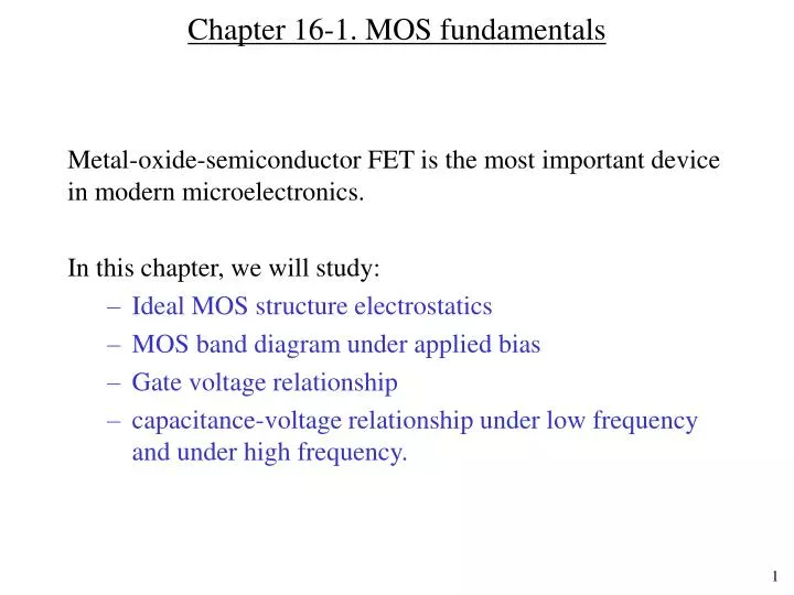
Chapter 16-1. MOS fundamentals. Metal-oxide-semiconductor FET is the most important device in modern microelectronics. In this chapter, we will study: Ideal MOS structure electrostatics MOS band diagram under applied bias Gate voltage relationship

E N D
Chapter 16-1. MOS fundamentals • Metal-oxide-semiconductor FET is the most important device in modern microelectronics. • In this chapter, we will study: • Ideal MOS structure electrostatics • MOS band diagram under applied bias • Gate voltage relationship • capacitance-voltage relationship under low frequency and under high frequency.
MOSFET N-channel MOSFET (NMOS) uses p-type substrate electrons P-Si
Pinch-off ID VD MOSFET operation VG3 VG2 VG3 > VG2 > VG1 VG1 When a positive voltage VG is applied to the gate relative to the substrate, mobile negative charges (electrons) gets attracted to Si-oxide interface. These induced electrons form the channel. For a given value of VG, the current ID increases with VD, and finally saturates.
Ideal MOS capacitor Let us consider a simple MOS capacitor and call it “ideal” • Oxide has zero charge, and no current can pass through it. • No charge centers are present in the oxide or at the oxide-semiconductor interface. • Semiconductor is uniformly doped • M = S • = + (EC – EF)FB
Effect of an applied bias • Let us ground the semiconductor and start applying different voltages, VG, to the gate • VG can be positive, negative or zero with respect to the semiconductor • EF, metal – EF, semiconductor = – qVG • (Since electron energy = q V, when V < 0, electron energy increases) • Since oxide has no charge, d Eoxide / dx = / = 0; i.e. the E-field inside the oxide is constant.
Consider p-type Si, apply VG < 0 Negative voltage attracts holes to the Si-oxide interface. This is called accumulation condition. Ei – EF should increases near the surface of Si. Accumulation of holes EC Ei EFs EV The oxide energy band has constant slope as shown. No current flows in Si EF in Si is constant.
Accumulation condition, VG < 0, p-type Si p-type Si M O VG < 0 charge density small Accumulation of holes near silicon surface, and electrons near the metal surface. Similar to a parallel plate capacitor structure. Sheet of holes + + x Sheet of electrons –––– x
x Consider p-type Si, apply VG > 0 (Depletion condition) Finite depletion layer width Depletion + + + EC • - - - • - - - Ei EFs EV EFM M O S
Consider p-Si, apply VG >> 0 (Inversion condition) Immobile acceptors + + + + EC Ei - - - - - - - - - - - - - - EFS - - EV Mobile electrons EFM EFM x
Inversion condition If we continue to increase the positive gate voltage, the bands at the semiconductor bends more strongly. At sufficiently high voltage, Ei can be below EF indicating large concentration of electrons in the conduction band. We say the material near the surface is “inverted”. The “inverted” layer is not gotten by doping, but by applying E-field. Where did we get the electrons from? When Ei(surface) – Ei(bulk) = 2 [EF – Ei(bulk)], the condition is start of “inversion”, and the voltage VG applied to gate is called VT(threshold voltage). For VG > VT, the Si surface is inverted.
Energy band diagrams and charge density diagrams describing MOS capacitor in n-type Si
Energy band diagrams and charge density diagrams describing MOS capacitor in p-type Si
Example 1 Construct line plots that visually identify the voltage ranges corresponding to accumulation, depletion and inversion in ideal n-type Si (i.e. p-channel) and p-type Si (i.e. n-channel) MOS devices. Answer: