Download
1 / 14
170 likes | 869 Views
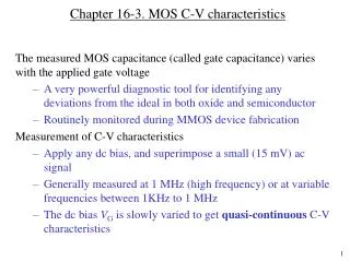
Chapter 16-3. MOS C-V characteristics. The measured MOS capacitance (called gate capacitance) varies with the applied gate voltage A very powerful diagnostic tool for identifying any deviations from the ideal in both oxide and semiconductor Routinely monitored during MMOS device fabrication

E N D
Chapter 16-3. MOS C-V characteristics • The measured MOS capacitance (called gate capacitance) varies with the applied gate voltage • A very powerful diagnostic tool for identifying any deviations from the ideal in both oxide and semiconductor • Routinely monitored during MMOS device fabrication • Measurement of C-V characteristics • Apply any dc bias, and superimpose a small (15 mV) ac signal • Generally measured at 1 MHz (high frequency) or at variable frequencies between 1KHz to 1 MHz • The dc bias VG is slowly varied to get quasi-continuous C-V characteristics
CG VG p-type C-V characteristics of MOS-capacitor on p- and n-type Si CG VG n-type The C-V data depends on the measurement frequency as well. The dotted line represents the low-frequency C-V data.
Measured C-V characteristics on an n-type Si ND = 9.0 1014 cm3 xox = 0.119 m
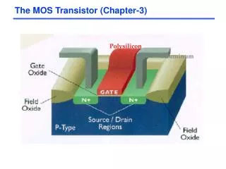
Accumulation of holes x MOS-capacitor under accumulation M O S Consider p-type Si under accumulation. VG < 0. Looks similar to parallel plate capacitor. CG = Cox where Cox = (oxA) / xox p-Si VG < 0 Thus, for all accumulation conditions, the gate capacitance is equal the oxide capacitance.
QM W Cox Cs Depletion of holes MOS-capacitor under depletion M O S Depletion condition: VG > 0 p-type Si VG > 0 CG is Cox in series with Cs where Cs can be defined as “semiconductor capacitance” Cox=ox A / xox Cs = Si A / W CG = Cox Cs/(Cox + CS) where s is surface potential In this case, the gate capacitance decreases as the gate voltage is increased. Why?
M O S p-Si VG >>0 QM W Depletion of holes Cox Cs Inversion electrons - function MOS-capacitor under inversion VG = VT and VG > VT Inversion condition s = 2 F At high frequency, inversion electrons are not able to respond to ac voltage. So, to balance the charge on the metal, the depletion layer width will vary with the ac. Cox=ox A/xox Cs = Si A/WT CG ( ) = Cox Cs / (Cox + CS) So, CG will be constant for VG VT
MOS-capacitor under inversion At low frequency, the inversion electrons will be able to respond to the ac voltage (Why?). So, the gate capacitance will be equal to the “oxide capacitance” (similar to a parallel plate capacitance). CG ( 0) = Cox = ox A / xox CG Low frequency Cox For VG > VT, the high frequency capacitance remains constant. Why? Cox Cs / (Cox+Cs) High frequency VG VT Study exercise 16.4 in text p-type Si
Example 1 Consider n-type silicon doped with NA=1016 cm3. The oxide thickness is 100 nm. Plot the CG vs. VG characteristics when VG is varied slowly from 5 V to +5 V. Assume MOS has area of 1 cm2. Find Cox. Find Cs (min) when W = WT (Note that Cs decreases as the depletion layer width increases. It is minimum when the depletion layer width is maximum, i.e. when W = WT). CG(min) = (3.47108 3.35) / (3.47+3.35) F = 1.7 108 F
CG 34.7nF low-f 17nF high-f VG 2.17 V p-type Example 1 (continued) = 2.15 V Plot the C-V characteristics 34.7 nF Explain why CG does not vary for VG > VT Question: How will you calculate CG when VG = 1V? Answer: Calculate s when VG = 1V using the eqn. above. From s find W, then calculate Cs. Then, calculate CG = (Cox Cs) / (Cox + Cs)
MOS-capacitor characteristics: Deep depletion The previous discussions pertain to the condition when the gate voltage is rampedslowly, from accumulation condition to depletion and then to inversion condition. When the ramp rate is high, the inversion layer does not form and does not have time to equilibrate. This is called “deep depletion” condition. In this case, W will continue to increase beyond WT and CG will continue to decrease as shown when the dc bias is varied from accumulation bias to deep depletion bias. To calculate W under deep depletion condition, invert the VG versus s relationship. Solve for s1/2 and hence s. Then, calculate W using W versus s relationship.
Some observations • VT = gate voltage required for start of inversion • = (+) for p-type Si • = () for n-type Si (+) - for p-type Si () - for n-type Si (+) () • Higher the doping, higher the |VT| value • Cmax = Cox and Cmin = CoxCs / (Cox + Cs) • Lower the doping, lower Cs and hence lower Cmin
Doping dependence of MOS-capacitor high frequency C-V characteristics, with xox = 0.1m
MOS-capacitor under deep depletion n-type Si Cs = Si A / W Cox=ox A / xox CG = Cox Cs / (Cox + Cs)
Not under steady state CG 34.7 nF 12 nF VG 5V 2.15 V Example 2 Consider example 1. Plot C-V characteristics if VG is varied from 5 V to + 5 V rapidly. CG (5 V) = Cox=34.7 nF, as before. CG (VG = VT) = 17 nF, as before. CG (VG > VT) will continue to reduce (unlike the quasi-steady state condition of example 1). When VG = 5 V, Solving for s , we get s = 2.38 V W = 0.545 m; Cs = 18.3 nF; CG= 12 nF