Chapter 2 Modern CMOS technology
Chapter 2 Modern CMOS technology. Introduction. CMOS process flow. NE 343: Microfabrication and thin film technology Instructor: Bo Cui, ECE, University of Waterloo; http://ece.uwaterloo.ca/~bcui/ Textbook: Silicon VLSI Technology by Plummer, Deal and Griffin.

Chapter 2 Modern CMOS technology
E N D
Presentation Transcript
Chapter 2 Modern CMOS technology Introduction. CMOS process flow. NE 343: Microfabrication and thin film technology Instructor: Bo Cui, ECE, University of Waterloo; http://ece.uwaterloo.ca/~bcui/ Textbook: Silicon VLSI Technology by Plummer, Deal and Griffin
CMOS: complementary metal–oxide–semiconductor • In the simplest CMOS technologies, we need to realize simply NMOS and PMOS transistors for circuits like those illustrated below. • Typical CMOS technologies in manufacturing add additional steps to implement multiple device VTH, thin film transistors (TFT) in SRAMs, capacitors for DRAMs etc. • CMOS described here requires 16 masks (through metal level 2) and >100 process steps. • There are many possible variations on the process flow (e.g. LOCOS device isolation vs. shallow trench isolation). n-MOS & p-MOS require different channel background doping and source/drain region doping. In CMOS, the gate is no longer “metal”, it is heavily doped poly-crystalline Si with low resistance.
CMOS is required by logic circuits S D D S NOR: Output = IN1+IN2 Inverter: Output = Input Output = GND = 0 if any Input or both are +V = 1 CMOS (n-MOS & p-MOS) reduces static power dissipation. Because (e.g. for the inverter) there is no current flow from +V to GND since one of the MOS is always off. The same inverter logic can also be realized by replacing the top PMOS with a resistor R (ON NMOS << R << OFF NMOS), but current flows when NMOS is on.
N-MOSFET (field effect transistor) operation Inverted to n-type • Body (bulk Si) is commonly tied to ground (0V). • When the gate is at a low voltage: • P-type body is at low voltage, source-channel-drain is N+PN+. • If drain is positive bias (i.e. electrons flow from the source and ‘drained’ to the drain), the right side PN+ diode is in reverse bias. • Left side N+P is in zero-bias, as source is usually connected to the grounded bulk Si. • No current flows through the channel, transistor is OFF • When the gate is at a high voltage: • Positive charge on gate of MOS capacitor. • Negative charge attracted to the top surface just below the gate oxide. • Inverts a channel under gate to n-type, source-channel-drain is N+NN+. • Now current can flow through n-type silicon from source through channel to drain, transistor is ON.
P-MOSFET (field effect transistor) operation Body tied to high voltage (= source voltage, supply voltage). Gate low (grounded, which is lower than high voltage bulk Si): transistor is ON. Gate high (same as bulk Si): transistor is OFF. Since voltage has only a relative meaning. This is equivalent to the situation of: grounded body/bulk Si, grounded source, negative (< 0V) drain voltage (so holes flow from source and ‘drained’ to drain). Then transistor is ON when gate is negatively biased, and OFF when gate is grounded.
Transistors as switches We can view MOS transistors as electrically controlled switches, and voltage at gate controls path from source to drain.
CMOS inverter Inverter: Output = Input g=Input=0, NMOS is off, PMOS is on. Output=+V=1. When Input =1, Output=GND=0
CMOS NAND gate Output = 0 only when both Inputs are 1
Cross-section of the CMOS IC p This is what we are going to fabricate in this chapter.
Fabrication “toolkit” LPCVD: low pressure chemical vapor deposition. PECVD: plasma enhanced CVD. APCVD: atmospheric pressure CVD RIE: reactive ion etching DRIE: deep RIE. CMP: chemical mechanical polishing • Insulating Layers • Oxidation, nitridation • Deposition (LPCVD, PECVD, APCVD) • Selective doping of silicon • Diffusion (in-situ doping) • Ion implantation • Epitaxy (in-situ doping) • Material deposition (silicon, metals, insulators) • LPCVD • PECVD • Sputter deposition • Patterning of Layers • Lithography (UV, deep UV, e-beam & x-ray) • Etching of (deposited) material • Dry etches—plasma, RIE, sputter etch, DRIE • Wetetches—etch in liquids, CMP etc
Chapter 2 Modern CMOS technology Introduction. CMOS process flow. NE 343 Microfabrication and thin film technology Instructor: Bo Cui, ECE, University of Waterloo Textbook: Silicon VLSI Technology by Plummer, Deal and Griffin
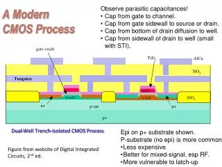
Choosing the substrate and active region formation Nitride has high tensile stress, oxide has compressive stress. The two stress can balance/compensate each other to reduce stress in Si that may cause defects in Si. LPCVD nitride: 3SiH4+4NH3 Si3N4+12H2, 800oC. LPCVD: low pressure chemical vapor deposition Substrate selection: moderately high resistivity (lightly doped, 1015cm-3), (100) orientation substrate (better Si/SiO2 interface than other orientations), P type. Start from low doping, then dope P-well and N-well by ion implantation that is much better controlled than substrate doping (done during crystal growth). Wafer cleaning, thermal oxidation (≈ 40 nm, using O2, or H2O generated from H2 and O2 reaction, cleaner than H2O vapor from boiling water), Si3N4 LPCVD (≈ 80 nm), photoresist spinning and baking (≈ 0.5 - 1.0 μm).
Active region formation Photolithography, nitride etching Mask #1 patterns the active areas. The nitride is dry etched. Dry etch = plasma etch, reactive species are generated in a plasma (like arc discharge). E.g F is generated in CF4 plasma. Atomic F is extremely reactive. Si3N4 + 12F 3SiF4 (gas/volatile, pumped away) + 2N2
LOCOS isolation LOCOS: LOCal Oxidation of Silicon Remove resist, thermal oxidation Si3N4 is very dense material and prevents/blocks H2O or O2 from diffusion to the Si surface, thus no oxidation under nitride. Remove photoresist. Field oxide is grown using a LOCOS process. Typically 90min @ 1000˚C in H2O grows SiO2 ≈ 0.5 µm. Field oxide is partially recessed into the surface (oxidation consume some of the silicon) Field oxides forms a lateral extension under the nitride layer – bird’s beak region Bird’s beak region limits device scaling and device density in VLSI circuits! http://en.wikipedia.org/wiki/LOCOS
Alternative process to LOCOS isolation: shallow trench isolation with filled implants (here P+) LOCOS: Bird’s Beak problem, unsuitable for small device. • Growth of pad silicon dioxide and deposition of silicon nitride as in LOCOS • Implant trench to increase field threshold (for better device isolation) and growth of liner oxide for passivation and smoothing • Trench fill with deposited oxide (not thermally grown oxide) • CMP (chemical mechanical polishing) for planarization. Note: this process added P+ impanation, slightly different from the process in textbook.
P-well formation Wet etch away Si3N4, spin photoresist, lithography, B+ implantation. In ion implantation, positive B+ ions are formed by exposing the source gas containing B to an arc discharge. Only B + is selected by a bending magnet to pass through a slit. B + energy is high enough to pass through the field (LOCOS) oxide. But photoresist is thick enough to block the ions. Mask #2 blocks a B+implant to form the wells for the NMOS devices. Typically dose 1013cm-2@ 150-200 KeV (very high energy). (Implant dose is in cm-2, doping concentration is in cm-3)
N-well formation Strip photoresist, spin resist and photolithography, ion implantation Mask #3 blocks a P+ implant to form the wells for the PMOS devices. Typically 1013 cm-2@ 300-400 KeV. (P is heavier than B, so higher energy needed)
N- and P- well formation Remove resist and anneal Ion energy is 100keV, much higher than energy needed to break 4 Si bonds (total 12eV), so ion implantation induces many damages. B and P have similar diffusion coefficient, so similar final well depth. A high temperature drive-in produces the “final” well depths and repairs implant damage. Typically 4-6 hours @ 1000˚C - 1100˚C or equivalent Dt. (here D is diffusion coefficient, t is time)
Threshold voltage (VTH) adjustment Spin photoresist, photolithography, B+ ion implantation Implant dose Figure 2-22 Mask #4 is used to mask the PMOS devices. A VTH adjust implant is done on the NMOS devices. Typically 1-5 x 1012cm-2 B+ implant @ 50 - 75 KeV. Note: section 2.2.5 is skipped
Threshold voltage (VTH) adjustment Remove resist, then spin photoresist, photolithography, As+ ion implantation Again, adjust VTH by controlling implant dose QI. Mask #5 is used to mask the NMOS devices. A VTH adjust implant is done on the PMOS devices. Typically 1-5 x 1012 cm-2 As+ implant @ 75 - 100 KeV.