Download
1 / 52
520 likes | 579 Views
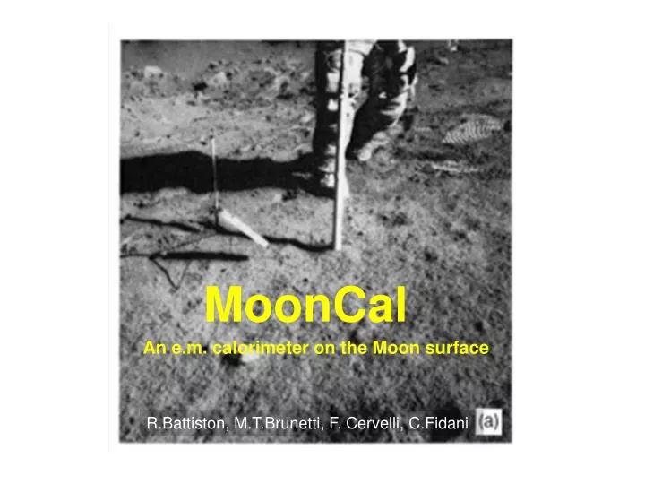
MoonCal. An e.m. calorimeter on the Moon surface. R.Battiston , M.T.Brunetti, F. Cervelli, C.Fidani. O graziosa luna, io mi rammento che, or volge l’anno, sovra questo colle io venia pien d’angoscia a rimirarti G. Leopardi. Physics Perpectives. Mooncal could :

E N D
MoonCal An e.m. calorimeter on the Moon surface R.Battiston, M.T.Brunetti, F. Cervelli, C.Fidani
O graziosa luna, io mi rammento che, or volge l’anno, sovra questo colle io venia pien d’angoscia a rimirarti G. Leopardi Physics Perpectives Mooncal could : Resolve the difference of electrons spectra proposed by the many diffusion models for sources in the TeV region from Vela, Cygnus loop and Monogem Detect an excess of positrons and electronsby the excellent energy resolution and the observations with high statistics Provide complementary observations on gamma’s with respect to Glast by a better energy resolution above 100 GeV. Targets : Galactic and extra-Galactic diffuse components, supernova remnants, pulsars, AGN’s, GRB’s Observe line gamma rays from SUSY particlesannihilation. As the energy resolution is better at higher energies,Mooncal will precisely measure the signature of line gamma rays
Simulation of Regolith Composition GEANT4 derives the Regolith Radiation Length (C0) from chemical composition and relative densities Regolith Radiation Length : 14.4 cm
Scintillator Geometry d = 7.5 cm r = 1 cm d = 7.5 cm L = 150 cm or L = 300 cm
MoonCal simulation: Boundary conditions and restrictions • CALORIMETER GEOMETRY: • Cylinder of 3 m radius and 1.5 m height filled with regolith and scintillators of 1 cm radius and 1.5 m height separated by 7.5 cm (on a xy grid). • ENERGY RESTRICTIONS: • Lower energy cut for gammas 550 keV • Lower energy cut for electrons and positrons 1.4 MeV • GEOMETRY RESTRICTIONS: • Incident angle: 45°≤q≤ 80° longitudinal containment • Incident area: inside a disk of 1 m radius lateral containment
Scintillator distance = 7.5 cmScintillator radius= 1 cm Distance vs Scintillator Diameter (1)
RESULTS The resolution E/E has been fitted according to:
Scintillator distance = 4 cmScintillator radius= 0.5 cm Distance vs Scintillator Diameter (2)
Low Energies Studies • Analysis Cuts: • First plot: resolution between 0.1 and 1 GeV with the following lower cuts: • Gammas, electrons, positrons 1 keV • -Second plot: resolution between 1 and 50 GeV with the following lower cuts: • Gammas 2 keV, electrons 356 keV, positrons 347 keV
metal Q = Q1 + Q2 = 2*Q1 substrate SiPM concept GM-APD gives no information on light intensity first proposed by Golovin and Sadygov in the mid ’90 SiPM • A single GM-APD is segmented in tiny • microdiodes connected in parallel, • each with the quenching resistance. • Each element is independent and gives the • same signal when fired by a photon • output signal is proportional to the number of triggered cells that for PDE=1 is the number of photons
Features of a SiPM • The characteristics of a SiPM are: • capability to detect extremely low photon fluxes (from 1 to few • hundred) giving a proportional information; • extremely fast response (determined by avalanche discharge): • in the order of few hundreds of ps. • Other features are: • Low bias voltage (20-60V) • Low power consumption • Insensitive to magnetic fields • Compact and rugged
SiPM @ ITC-irst First prototypes The wafer includes many structure differing in geometrical details 1mm 1mm The basic SiPM geometry is composed by 25x25 cells Cell size: 40x40mm2
40 cm of regolith T=-20 ± 3 C Regolith Physical Properties
Further Developments Longitudinal segmentation of Scintillator Rods Steps: 5 or 10 cm
Numbers and Weight as a CONCLUSION Area covered by a single rod Surfice covered by Moon Cal d = 4 cm Area ~ 7 cm2~28 m2 d = 7.5 cm Area ~ 24 cm2 d = 15 cm Area ~ 97 cm2 Scintillator rod : Wrapping in Carbon fiber Weight of a single rod (length: 150 cm): r=0.5 cm .15 Kg r= 1cm .5 Kg
Properties of a SiPM The properties described for the GM-APD are valid for the SiPM with two additional complications: 1) Further term in the photodetection efficiency: PDE = Npulses / Nphotons = QE x P01 x Ae Ae = (Active area) / (total SiPM area) Dead area is given by the structures at the edges of the microcell (metal layers, trenches, resistor…)
cell1 cell2 cell1 cell2 Properties of a SiPM • 2)Optical cross-talk • During an avalanche discharge photons are emitted. • 3x10⁻⁵ photons with energy higher than 1.14eV emitted • per carrier crossing the junction. • [from A. Lacaita et al., IEEE TED, vol. 40, n. 3, 1993:] • Those photons can trigger the • avalanche in an adjacent cell: • optical cross-talk. • Solutions: • operate at low over-voltage => low gain => few photons emitted • optical isolation structure:
SiPM manufacturers • Russian groups: • Obninsk/CPTA, Moscow (Golovin) • Mephi/PULSAR, Moscow (Dolgoshein) • JINR, Dubna (Sadygov) • They have been working on this since the beginning. • New labs/companies involved in SiPM production: • ITC-irst • Hamamatsu • SensL • MPI
SiPM @ ITC-irst • Development of SiPM is done in the framework of an • agreement between INFN and ITC called MEMS: • role of ITC-irst: • toproduce a matrix of SiPMs with detection efficiency • optimized in the short-wavelength region. • role of INFN (Pisa, Perugia, Bologna, Bari, Trento): • to couple the SiPM with a scintillator, to develop a read-out • electronics for calorimetry, PET, TOF applications. • Project started at the beginning of 2005. • Details on the status of the project: • http://sipm.itc.it
First production Completed in september 2005. Characteristics of the first fabrication run: 1) 11 photolithografic masks 180 process steps (3 months in clean room) 2) Substrate: p-type epitaxial, 4mm thick 3) Quenching resistance made of doped polysilicon 4) No structure for optical isolation 5) Geometry not optimized for maximum PDE Main objective was to study the breakdown properties!
Electrical characterization IV characteristics of 10 devices T=22oC position of the tested devices • Breakdown voltage 31V • Uniform VBD all over the wafer surface
Signal characteristics SiPMread-out by means of a wide-band voltage amplifier on a scope Dark signal double signal (optical cross-talk) single cell signal VBIAS=35.5V Single signal @ 32.5, 34 and 35.5V Rise time ~1ns Recovery time ~70ns
Single electron spectrum Single electron spectrum in dark condition Integration time = 100ns. 35V 34V 33V
Gain Gain vs Bias voltage T=22oC Linear dependence, as expected. Q=Cmicrocell*(Vbias-Vbreakdown) => C = 80-90fF
Preliminary optical characterization Example of a Signal Response to light excitation (l=470nm) VBIAS=33.5V T=22oC No measurement of PDE has been done yet. Dark signals Trigger from pulse gen. bunch of photons