Tech Evolution: Impact of Moore's Law on Memory Technology
Explore the impact of Moore's Law on memory technology, including the basics of memory hierarchy, SRAM and DRAM, magnetic disks, and implications for future systems. Discover the exponential growth curve of computer performance and memory capacities, and how it shapes the future of technology. Uncover the challenges and opportunities in advancing technology, and the significance of adhering to Moore's Law. Delve into the anatomy of SRAM and DRAM cells, their functionalities, and the addressing arrays in memory systems.

Tech Evolution: Impact of Moore's Law on Memory Technology
E N D
Presentation Transcript
Memory TechnologyOct 5, 2000 15-213 • Topics • Memory Hierarchy Basics • Static RAM • Dynamic RAM • Magnetic Disks • Access Time Gap class12.ppt
Impact of Technology • Moore’s Law • Observation by Gordon Moore, Intel founder, in 1971 • Transistors / Chip doubles every 18 months • Has expanded to include processor speed, disk capacity, … • We Owe a Lot to the Technologists • Computer science has ridden the wave • Things Aren’t Over Yet • Technology will continue to progress along current growth curves • For at least 7–10 more years • Difficult technical challenges in doing so • Even Technologists Can’t Beat Laws of Physics • Quantum effects create fundamental limits as approach atomic scale • Opportunities for new devices
Impact of Moore’s Law • Moore’s Law • Performance factors of systems built with integrated circuit technology follow exponential curve • E.g., computer speed / memory capacities double every 1.5 years • Implications • Computers 10 years from now will run 100 X faster • Problems that appear intractable today will be straightforward • Must not limit future planning with today’s technology • Example Application Domains • Speech recognition • Will be routinely done with handheld devices • Breaking secret codes • Need to use large enough keys • Digital Video • Will stream just like today’s MP3’s
Computer System Processor Reg Cache Memory-I/O bus I/O controller I/O controller I/O controller Memory Display Network Disk Disk
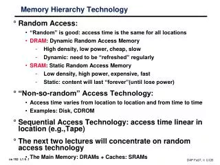
CPU C a c h e regs Levels in Memory Hierarchy cache virtual memory Memory disk 8 B 32 B 8 KB Register Cache Memory Disk Memory size: speed: $/Mbyte: block size: 200 B 2 ns 8 B 32KB - 4MB 4 ns $100/MB 32 B 128 MB 60 ns $1.50/MB 8 KB 30 GB 8 ms $0.05/MB larger, slower, cheaper
1 cm 1 mm 0.1 mm 10µm 1 µm 0.1 µm 10 nm 1 nm 1 Å Dimensions 2000 devices (0.18 µm) Chip size (1 cm) Diameter of Human Hair (25 µm) 1996 devices (0.35 µm) 2007 devices (0.1 µm) Silicon atom radius (1.17 Å) Deep UV Wavelength (0.248 µm) X-ray Wavelength (0.6 nm)
Scaling to 0.1µm • Semiconductor Industry Association, 1992 Technology Workshop • Projected future technology based on past trends • 199219951998200120042007 • Feature size (µm ): 0.5 0.35 0.25 0.18 0.12 0.10 • Industry is slightly ahead of projection • DRAM capacity: 16M 64M 256M 1G 4G 16G • Doubles every 1.5 years • Prediction on track • Chip area (cm2):2.5 4.0 6.0 8.0 10.0 12.5 • Way off! Chips staying small
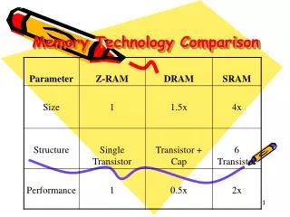
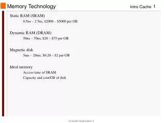
Static RAM (SRAM) • Fast • ~4 nsec access time • Persistent • as long as power is supplied • no refresh required • Expensive • ~$100/MByte • 6 transistors/bit • Stable • High immunity to noise and environmental disturbances • Technology for caches
bit line bit line Stable Configurations b b’ word line (6 transistors) 0 1 1 0 Anatomy of an SRAM Cell Terminology: bit line: carries data word line: used for addressing • Write: • 1. set bit lines to new data value • b’ is set to the opposite of b • 2. raise word line to “high” • sets cell to new state (may involve flipping relative to old state) • Read: • 1. set bit lines high • 2. set word line high • 3. see which bit line goes low
1 0.9 0.8 0.7 0.6 0.5 V1 0.4 V2 0.3 0.2 Vin 0.1 V1 0 0 0.2 0.4 0.6 0.8 1 V2 Vin SRAM Cell Principle • Inverter Amplifies • Negative gain • Slope < –1 in middle • Saturates at ends • Inverter Pair Amplifies • Positive gain • Slope > 1 in middle • Saturates at ends
Vin V1 V2 1 0.9 0.8 0.7 0.6 0.5 Vin 0.4 V2 0.3 0.2 0.1 0 0 0.2 0.4 0.6 0.8 1 Vin Bistable Element • Stability • Require Vin = V2 • Stable at endpoints • recover from pertubation • Metastable in middle • Fall out when perturbed • Ball on Ramp Analogy Stable Metastable Stable
Address decoder A0 A1 A2 A3 Example SRAM Configuration (16 x 8) b7 b7’ b1 b1’ b0 b0’ W0 W1 memory cells W15 R/W sense/write amps sense/write amps sense/write amps Input/output lines d7 d1 d0
Dynamic RAM (DRAM) • Slower than SRAM • access time ~60 nsec • Not persistent • every row must be accessed every ~1 ms (refreshed) • Cheaper than SRAM • ~$1.50 / MByte • 1 transistor/bit • Fragile • electrical noise, light, radiation • Workhorse memory technology
Reading Word Line Bit Line V ~ Cnode / CBL Anatomy of a DRAM Cell Word Line Bit Line Storage Node Access Transistor Cnode CBL Writing Word Line Bit Line V Storage Node
c r Addressing Arrays with Bits • Array Size • R rows, R = 2r • C columns, C = 2c • N = R * C bits of memory • Addressing • Addresses are n bits, where N = 2n • row(address) = address / C • leftmost r bits of address • col(address) = address % C • rightmost bits of address • Example • R = 2 • C = 4 • address = 6 row col address = n 0 1 2 3 0 000 001 010 011 1 100 101 110 111 col 2 row 1
8 \ 8 \ Example 2-Level Decode DRAM (64Kx1) RAS 256 Rows Row decoder 256x256 cell array Row address latch row 256 Columns A7-A0 column sense/write amps R/W’ col Provide 16-bit address in two 8-bit chunks Column address latch column latch and decoder CAS Dout Din
DRAM Operation • Row Address (~50ns) • Set Row address on address lines & strobe RAS • Entire row read & stored in column latches • Contents of row of memory cells destroyed • Column Address (~10ns) • Set Column address on address lines & strobe CAS • Access selected bit • READ: transfer from selected column latch to Dout • WRITE: Set selected column latch to Din • Rewrite (~30ns) • Write back entire row
Observations About DRAMs • Timing • Access time (= 60ns) < cycle time (= 90ns) • Need to rewrite row • Must Refresh Periodically • Perform complete memory cycle for each row • Approximately once every 1ms • Sqrt(n) cycles • Handled in background by memory controller • Inefficient Way to Get a Single Bit • Effectively read entire row of Sqrt(n) bits
RAS Row decoder 256x256 cell array Row address latch 8 \ row A7-A0 sense/write amps R/W’ col Column address latch column latch and decoder 8 \ CAS Enhanced Performance DRAMs • Conventional Access • Row + Col • RAS CAS RAS CAS ... • Page Mode • Row + Series of columns • RAS CAS CAS CAS ... • Gives successive bits • Other Acronyms • EDORAM • “Extended data output” • SDRAM • “Synchronous DRAM” Entire row buffered here Typical Performance row access time col access time cycle time page mode cycle time 50ns 10ns 90ns 25ns
256x256 cell array column sense/write amps Shift Register Video RAM • Performance Enhanced for Video / Graphics Operations • Frame buffer to hold graphics image • Writing • Random access of bits • Also supports rectangle fill operations • Set all bits in region to 0 or 1 • Reading • Load entire row into shift register • Shift out at video rates • Performance Example • 1200 X 1800 pixels / frame • 24 bits / pixel • 60 frames / second • 2.8 GBits / second Video Stream Output
DRAM Driving Forces • Capacity • 4X per generation • Square array of cells • Typical scaling • Lithography dimensions 0.7X • Areal density 2X • Cell function packing 1.5X • Chip area 1.33X • Scaling challenge • Typically Cnode / CBL = 0.1–0.2 • Must keep Cnode high as shrink cell size • Retention Time • Typically 16–256 ms • Want higher for low-power applications
Plate Area A Dielectric Material Dielectric Constant d C = A/d DRAM Storage Capacitor • Planar Capacitor • Up to 1Mb • C decreases linearly with feature size • Trench Capacitor • 4 Mb –1 Gb • Lining of hole in substrate • Stacked Cell • 1Gb • On top of substrate • Use high dielectric
SiO2 Dielectric Storage Plate Reference Plate Trench Capacitor • Process • Etch deep hole in substrate • ~5 µm deep • ~0.5 µm diameter • Becomes reference plate • Grow oxide on walls • Dielectric • Fill with polysilicon plug • Tied to storage node
IBM DRAM Cell • IBM J. R&D, Jan/Mar ‘95 • Evolution from 4 – 256 Mb 4 Mb Cell Structure
Cell Layouts 4Mb 16Mb 64Mb 256Mb IBM DRAM Evolution • IBM J. R&D, Jan/Mar ‘95 • Evolution from 4 – 256 Mb • 256 Mb uses cell with area 0.6 µm2 Relative Sizes
Mitsubishi Stacked Cell DRAM • IEDM ‘95 • Claim suitable for 1 – 4 Gb • Technology • 0.14 µm process • 8 nm gate oxide • 0.29 µm2 cell • Storage Capacitor • Fabricated on top of everything else • Rubidium electrodes • High dielectric insulator • 50X higher than SiO2 • 25 nm thick • Cell capacitance 25 femtofarads Cross Section of 2 Cells
Magnetic Disks Disk surface spins at 3600–15,000 RPM read/write head arm The surface consists of a set of concentric magnetized rings called tracks The read/write head floats over the disk surface and moves back and forth on an arm from track to track. Each track is divided into sectors
Disk Capacity • Parameter 18GB Example • Number Platters 12 • Surfaces / Platter 2 • Number of tracks 6962 • Number sectors / track 213 • Bytes / sector 512 • Total Bytes 18,221,948,928
Disk Operation • Operation • Read or write complete sector • Seek • Position head over proper track • Typically 6-9ms • Rotational Latency • Wait until desired sector passes under head • Worst case: complete rotation 10,025 RPM 6 ms • Read or Write Bits • Transfer rate depends on # bits per track and rotational speed • E.g., 213 * 512 bytes @10,025RPM = 18 MB/sec. • Modern disks have external transfer rates of up to 100 MB/sec
Disk Performance • Getting First Byte • Seek + Rotational latency = 7,000 – 19,000 µsec • Getting Successive Bytes • ~ 0.06 µsec each • roughly 100,000 times faster than getting the first byte! • Optimizing Performance: • Large block transfers are more efficient • Try to do other things while waiting for first byte • switch context to other computing task • processor is interrupted when transfer completes
Disk / System Interface (1) Initiate Sector Read • 1. Processor Signals Controller • Read sector X and store starting at memory address Y • 2. Read Occurs • “Direct Memory Access” (DMA) transfer • Under control of I/O controller • 3. I/O Controller Signals Completion • Interrupts processor • Can resume suspended process Processor Reg (3) Read Done Cache Memory-I/O bus (2) DMA Transfer I/O controller Memory Disk Disk
Magnetic Disk Technology • Seagate ST-12550N Barracuda 2 Disk • Linear density 52,187. bits per inch (BPI) • Bit spacing 0.5 µm • Track density 3,047. tracks per inch (TPI) • Track spacing 8.3 µm • Total tracks 2,707. tracks • Rotational Speed 7200. RPM • Avg Linear Speed 86.4 kilometers / hour • Head Floating Height 0.13 microns • Analogy: • put the Sears Tower on its side • fly it around the world, 2.5cm above the ground • each complete orbit of the earth takes 8 seconds
CD Read Only Memory (CDROM) • Basis • Optical recording technology developed for audio CDs • 74 minutes playing time • 44,100 samples / second • 2 X 16-bits / sample (Stereo) Raw bit rate = 172 KB / second • Add extra 288 bytes of error correction for every 2048 bytes of data • Cannot tolerate any errors in digital data, whereas OK for audio • Bit Rate • 172 * 2048 / (288 + 2048) = 150 KB / second • For 1X CDROM • N X CDROM gives bit rate of N * 150 • E.g., 12X CDROM gives 1.76 MB / second • Capacity • 74 Minutes * 150 KB / second * 60 seconds / minute = 650 MB
metric 1980 1985 1990 1995 2000 2000:1980 $/MB 19,200 2,900 320 256 100 190 access (ns) 300 150 35 15 2 100 SRAM metric 1980 1985 1990 1995 2000 2000:1980 $/MB 8,000 880 100 30 1.5 5,300 access (ns) 375 200 100 70 60 6 typical size(MB) 0.064 0.256 4 16 64 1,000 DRAM metric 1980 1985 1990 1995 2000 2000:1980 $/MB 500 100 8 0.30 0.05 10,000 access (ms) 87 75 28 10 8 11 typical size(MB) 1 10 160 1,000 9,000 9,000 Disk Storage Trends (Culled from back issues of Byte and PC Magazine)
Processor clock rates Processors metric 1980 1985 1990 1995 2000 2000:1980 typical clock(MHz) 1 6 20 150 750 750 processor 8080 286 386 Pentium P-III culled from back issues of Byte and PC Magazine
Memory Technology Summary • Cost and Density Improving at Enormous Rates • Speed Lagging Processor Performance • Memory Hierarchies Help Narrow the Gap: • Small fast SRAMS (cache) at upper levels • Large slow DRAMS (main memory) at lower levels • Incredibly large & slow disks to back it all up • Locality of Reference Makes It All Work • Keep most frequently accessed data in fastest memory