Memory Hierarchy Technology
250 likes | 523 Views
Memory Hierarchy Technology. Random Access: “Random” is good: access time is the same for all locations DRAM : Dynamic Random Access Memory High density, low power, cheap, slow Dynamic: need to be “refreshed” regularly SRAM : Static Random Access Memory

Memory Hierarchy Technology
E N D
Presentation Transcript
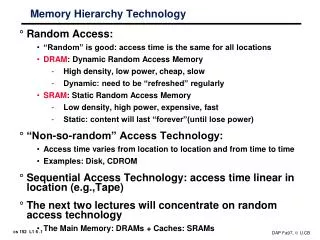
Memory Hierarchy Technology • Random Access: • “Random” is good: access time is the same for all locations • DRAM: Dynamic Random Access Memory • High density, low power, cheap, slow • Dynamic: need to be “refreshed” regularly • SRAM: Static Random Access Memory • Low density, high power, expensive, fast • Static: content will last “forever”(until lose power) • “Non-so-random” Access Technology: • Access time varies from location to location and from time to time • Examples: Disk, CDROM • Sequential Access Technology: access time linear in location (e.g.,Tape) • The next two lectures will concentrate on random access technology • The Main Memory: DRAMs + Caches: SRAMs
Main Memory Background • Performance of Main Memory: • Latency: Cache Miss Penalty • Access Time: time between request and word arrives • Cycle Time: time between requests • Bandwidth: I/O & Large Block Miss Penalty (L2) • Main Memory is DRAM: Dynamic Random Access Memory • Dynamic since needs to be refreshed periodically (8 ms) • Addresses divided into 2 halves (Memory as a 2D matrix): • RAS or Row Access Strobe • CAS or Column Access Strobe • Cache uses SRAM: Static Random Access Memory • No refresh (6 transistors/bit vs. 1 transistor /bit) • Address not divided • Size: DRAM/SRAM 4-8, Cost/Cycle time: SRAM/DRAM 8-16
Random Access Memory (RAM) Technology • Why do computer designers need to know about RAM technology? • Processor performance is usually limited by memory bandwidth • As IC densities increase, lots of memory will fit on processor chip • Tailor on-chip memory to specific needs • Instruction cache • Data cache • Write buffer • What makes RAM different from a bunch of flip-flops? • Density: RAM is much more denser
Static RAM Cell 6-Transistor SRAM Cell word word (row select) • Write: 1. Drive bit lines (bit=1, bit=0) 2.. Select row • Read: 1. Precharge bit and bit to Vdd 2.. Select row 3. Cell pulls one line low 4. Sense amp on column detects difference between bit and bit 0 1 0 1 bit bit bit bit replaced with pullup to save area
Wr Driver & Precharger Wr Driver & Precharger Wr Driver & Precharger Wr Driver & Precharger - + - + - + - + - + - + - + - + Sense Amp Sense Amp Sense Amp Sense Amp Typical SRAM Organization: 16-word x 4-bit Din 3 Din 2 Din 1 Din 0 WrEn Precharge A0 Word 0 SRAM Cell SRAM Cell SRAM Cell SRAM Cell A1 Address Decoder A2 Word 1 SRAM Cell SRAM Cell SRAM Cell SRAM Cell A3 : : : : Word 15 SRAM Cell SRAM Cell SRAM Cell SRAM Cell Q: Which is longer: word line or bit line? Dout 3 Dout 2 Dout 1 Dout 0
A N 2 words N x M bit SRAM WE_L OE_L D M Logic Diagram of a Typical SRAM • Write Enable is usually active low (WE_L) • Din and Dout are combined to save pins: • A new control signal, output enable (OE_L) is needed • WE_L is asserted (Low), OE_L is disasserted (High) • D serves as the data input pin • WE_L is disasserted (High), OE_L is asserted (Low) • D is the data output pin • Both WE_L and OE_L are asserted: • Result is unknown. Don’t do that!!! • Although could change VHDL to do what desire, must do the best with what you’ve got (vs. what you need)
A N 2 words N x M bit SRAM WE_L OE_L D M Typical SRAM Timing Write Timing: Read Timing: High Z D Data In Data Out Data Out Junk A Write Address Read Address Read Address OE_L WE_L Write Hold Time Read Access Time Read Access Time Write Setup Time
Problems with SRAM Select = 1 • Six transistors use up a lot of area • Consider a “Zero” is stored in the cell: • Transistor N1 will try to pull “bit” to 0 • Transistor P2 will try to pull “bit bar” to 1 • But bit lines are precharged to high: Are P1 and P2 necessary? P1 P2 Off On On On On Off N1 N2 bit = 1 bit = 0
1-Transistor Memory Cell (DRAM) • Write: • 1. Drive bit line • 2.. Select row • Read: • 1. Precharge bit line to Vdd • 2.. Select row • 3. Cell and bit line share charges • Very small voltage changes on the bit line • 4. Sense (fancy sense amp) • Can detect changes of ~1 million electrons • 5. Write: restore the value • Refresh • 1. Just do a dummy read to every cell. row select bit
Classical DRAM Organization (square) bit (data) lines • Row and Column Address together: • Select 1 bit a time r o w d e c o d e r Each intersection represents a 1-T DRAM Cell RAM Cell Array word (row) select Column Selector & I/O Circuits row address Column Address data
DRAM logical organization (4 Mbit) • Square root of bits per RAS/CAS Column Decoder … D Sense Amps & I/O 1 1 Q Memory Array A0…A1 0 (2,048 x 2,048) Storage W ord Line Cell
Memory Systems n address DRAM Controller DRAM 2^n x 1 chip n/2 Memory Timing Controller w Bus Drivers Tc = Tcycle + Tcontroller + Tdriver
Logic Diagram of a Typical DRAM RAS_L CAS_L WE_L OE_L • Control Signals (RAS_L, CAS_L, WE_L, OE_L) are all active low • Din and Dout are combined (D): • WE_L is asserted (Low), OE_L is disasserted (High) • D serves as the data input pin • WE_L is disasserted (High), OE_L is asserted (Low) • D is the data output pin • Row and column addresses share the same pins (A) • RAS_L goes low: Pins A are latched in as row address • CAS_L goes low: Pins A are latched in as column address • RAS/CAS edge-sensitive A 256K x 8 DRAM D 9 8
Key DRAM Timing Parameters • tRAC: minimum time from RAS line falling to the valid data output. • Quoted as the speed of a DRAM • A fast 4Mb DRAM tRAC = 60 ns • tRC: minimum time from the start of one row access to the start of the next. • tRC = 110 ns for a 4Mbit DRAM with a tRAC of 60 ns • tCAC: minimum time from CAS line falling to valid data output. • 15 ns for a 4Mbit DRAM with a tRAC of 60 ns • tPC: minimum time from the start of one column access to the start of the next. • 35 ns for a 4Mbit DRAM with a tRAC of 60 ns
RAS_L DRAM Write Timing RAS_L CAS_L WE_L OE_L • Every DRAM access begins at: • The assertion of the RAS_L • 2 ways to write: early or late v. CAS A 256K x 8 DRAM D 9 8 DRAM WR Cycle Time CAS_L A Row Address Col Address Junk Row Address Col Address Junk OE_L WE_L D Junk Data In Junk Data In Junk WR Access Time WR Access Time Early Wr Cycle: WE_L asserted before CAS_L Late Wr Cycle: WE_L asserted after CAS_L
RAS_L CAS_L WE_L OE_L A 256K x 8 DRAM D 9 8 RAS_L DRAM Read Timing • Every DRAM access begins at: • The assertion of the RAS_L • 2 ways to read: early or late v. CAS DRAM Read Cycle Time CAS_L A Row Address Col Address Junk Row Address Col Address Junk WE_L OE_L D High Z Junk Data Out High Z Data Out Read Access Time Output Enable Delay Early Read Cycle: OE_L asserted before CAS_L Late Read Cycle: OE_L asserted after CAS_L
Main Memory Performance • Simple: • CPU, Cache, Bus, Memory same width (32 bits) • Wide: • CPU/Mux 1 word; Mux/Cache, Bus, Memory N words (Alpha: 64 bits & 256 bits) • Interleaved: • CPU, Cache, Bus 1 word: Memory N Modules(4 Modules); example is word interleaved
Cycle Time versus Access Time Cycle Time • DRAM (Read/Write) Cycle Time >> DRAM (Read/Write) Access Time • 2:1; why? • DRAM (Read/Write) Cycle Time : • How frequent can you initiate an access? • Analogy: A little kid can only ask his father for money on Saturday • DRAM (Read/Write) Access Time: • How quickly will you get what you want once you initiate an access? • Analogy: As soon as he asks, his father will give him the money • DRAM Bandwidth Limitation analogy: • What happens if he runs out of money on Wednesday? Access Time Time
Increasing Bandwidth - Interleaving Access Pattern without Interleaving: CPU Memory D1 available Start Access for D1 Start Access for D2 Memory Bank 0 Access Pattern with 4-way Interleaving: Memory Bank 1 CPU Memory Bank 2 Memory Bank 3 Access Bank 1 Access Bank 0 Access Bank 2 Access Bank 3 We can Access Bank 0 again
Main Memory Performance • Timing model • 1 to send address, • 6 access time, 1 to send data • Cache Block is 4 words • Simple M.P. = 4 x (1+6+1) = 32 • Wide M.P. = 1 + 6 + 1 = 8 • Interleaved M.P. = 1 + 6 + 4x1 = 11
Independent Memory Banks • How many banks? number banks number clocks to access word in bank • For sequential accesses, otherwise will return to original bank before it has next word ready • Increasing DRAM => fewer chips => harder to have banks • Growth bits/chip DRAM : 50%-60%/yr • Nathan Myrvold M/S: mature software growth (33%/yr for NT) growth MB/$ of DRAM (25%-30%/yr)
N cols RAS_L Page Mode DRAM: Motivation Column Address • Regular DRAM Organization: • N rows x N column x M-bit • Read & Write M-bit at a time • Each M-bit access requiresa RAS / CAS cycle • Fast Page Mode DRAM • N x M “register” to save a row DRAM Row Address N rows M bits M-bit Output 1st M-bit Access 2nd M-bit Access CAS_L A Row Address Col Address Junk Row Address Col Address Junk
N cols Fast Page Mode Operation Column Address • Fast Page Mode DRAM • N x M “SRAM” to save a row • After a row is read into the register • Only CAS is needed to access other M-bit blocks on that row • RAS_L remains asserted while CAS_L is toggled DRAM Row Address N rows N x M “SRAM” M bits M-bit Output 1st M-bit Access 2nd M-bit 3rd M-bit 4th M-bit RAS_L CAS_L A Row Address Col Address Col Address Col Address Col Address
DRAM History • DRAMs: capacity +60%/yr, cost –30%/yr • 2.5X cells/area, 1.5X die size in 3 years • ‘97 DRAM fab line costs $1B to $2B • DRAM only: density, leakage v. speed • Rely on increasing no. of computers & memory per computer (60% market) • SIMM or DIMM is replaceable unit => computers use any generation DRAM • Commodity, second source industry => high volume, low profit, conservative • Little organization innovation in 20 years page mode, EDO, Synch DRAM • Order of importance: 1) Cost/bit 1a) Capacity • RAMBUS: 10X BW, +30% cost => little impact
Summary: • Two Different Types of Locality: • Temporal Locality (Locality in Time): If an item is referenced, it will tend to be referenced again soon. • Spatial Locality (Locality in Space): If an item is referenced, items whose addresses are close by tend to be referenced soon. • By taking advantage of the principle of locality: • Present the user with as much memory as is available in the cheapest technology. • Provide access at the speed offered by the fastest technology. • DRAM is slow but cheap and dense: • Good choice for presenting the user with a BIG memory system • SRAM is fast but expensive and not very dense: • Good choice for providing the user FAST access time.