2-1 Integrated Circuits
150 likes | 369 Views
2-1 Integrated Circuits. Integrated Circuits(IC) Digital circuits are constructed with Integrated Circuits An Integrated Circuits is a small silicon semiconductor crystal, called chip The various gates are interconnected inside the chip to form the required circuit

2-1 Integrated Circuits
E N D
Presentation Transcript
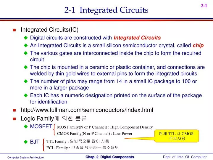
2-1 Integrated Circuits • Integrated Circuits(IC) • Digital circuits are constructed with Integrated Circuits • An Integrated Circuits is a small silicon semiconductor crystal, called chip • The various gates are interconnected inside the chip to form the required circuit • The chip is mounted in a ceramic or plastic container, and connections are welded by thin gold wires to external pins to form the integrated circuits • The number of pins may range from 14 in a small IC package to 100 or more in a larger package • Each IC has a numeric designation printed on the surface of the package for identification • http://www.fullman.com/semiconductors/index.html • Logic Family에 의한 분류 • MOSFET • BJT MOS Family(N or P Channel) : High Component Density CMOS Family(N or P Channel) : Low Power 현재 TTL 과 CMOS 주로사용 TTL Family : 일반적으로 많이 사용 ECL Family : 고속을 요구하는 특수용도
Pt Si • TTL Family • 54 Series : -55 ° C 125 °C, Military 74 Series : 0 ° C 70 ° C, Commercial • 54/74 : Standard • 54L/74L : Low-power • 54S/74S : Schottky • 54LS/74LS : Low-power, Schottky • 54H/74H : High-speed • CMOS Family • 4000 Series(RCA), MC14500(Motorola), 5000(Toshiba), 54C/74C Series, 54HC/74HC Series • 동작온도 : -30 ° C 85 ° C , Fan-out 증가, Noise Margin 증가, Low-power *Schottky Diode 금속과 반도체를 연결하면 ECL 보다는 느리지만 동작속도가 빨라짐( 0.4 Volt에서 동작) i V 0.2 0.4 0.6 Schottky Diode Schottky Transistor Forward Bias
Package Types • Small Outline Transistor (SOT) • Small Outline Package (SOP) • Dual-In-Line Package (DIP) • Plastic/Ceramic Pin Grid Array (PPGA/CPGA) • Plastic Leaded Chip Carrier (PLCC)
Ceramic Leadless Chip Carrier (LCC) • Plastic Quad Flat Package (PQFP) • TO Packages (Transistor single Outline)
2-2 Decoder/Encoder • Decoder • A combinational circuit that converts binary information from the n coded inputs to a maximum of 2n unique outputs • n-to-m line decoder = n x m decoder • n inputs, m outputs • If the n-bit coded information has unused bit combinations, the decoder may have less than 2n outputs • m 2n • 3-to-8 Decoder • Logic Diagram : Fig. 2-1 • Truth Table : Tab. 2-1 • Commercial decoders include one or more Enable Input(E) Fig. 2-1 3-to-8 Decoder D0 D1 D2 D3 D4 D5 D6 D7 A2 A1 A0 Tab. 2-1 Truth table for 3-to-8 Decoder Enable(E)
* Active Low Output * Fig. 2-1 3-to-8 Decoder 는 Active High Output • NAND Gate Decoder • Constructed with NAND instead of AND gates • Logic Diagram/Truth Table : Fig. 2-2 • Decoder Expansion • 3 X 8 Decoder constructed with two 2 X 4 Decoder • Constructed decoder : Fig. 2-3 • Encoder • Inverse Operation of a decoder • 2n input, n output • Truth Table : Tab. 2-2 • 3 OR Gates Implementation • A0 = D1 + D3 + D5 + D7 • A1 = D2 + D3 + D6 + D7 • A2 = D4 + D5 + D6 + D7 D0 D1 D2 D3 A0 A1 Fig. 2-2 2-to-4 Decoder with NAND gates Enable(E) (a) Truth Table (b) Logic Diagram A2 A1 A0 D0 D1 D2 D3 D4 D5 D6 D7 Tab. 2-2 Truth Table for Encoder Fig. 2-3 A 3-to-8 Decoder constructed with two with 2-to-4 Decoder
2-3 Multiplexers • Multiplexer(Mux) • A combinational circuit that receives binary information from one of 2n input data lines and directs it to a single output line • A 2n -to 1 multiplexer has 2n input data lines and n input selection lines(Data Selector) • 4-to-1 multiplexer Diagram : Fig. 2-4 • 4-to-1 multiplexer Function Table : Tab. 2-3 • Quadruple 2-to-1 Multiplexer • Quadruple 2-to-1 Multiplexer : Fig. 2-5 I0 I1 I2 I3 Y Tab. 2-3 Function Table for 4-to-1 line Multiplexter S0 S1 Fig. 2-4 4-to-1 Line Multiplexer Enable Select Quadruple 2 x 1 Mux A0 A1 A2 A3 Y0 Y1 Y2 Y3 Fig. 2-5 Quadruple 2-to-1 line Multiplexter B0 B1 B2 B3 (a) Function Table (b) Block Diagram
2-4 Registers • Register • A group of flip-flops with each flip-flop capable of storing one bit of information • An n-bit register has a group of n flip-flops and is capable of storing any binary information of n bits • The simplest register consists only of flip-flops, with no external gate : Fig. 2-6 • A clock input C will load all four inputs in parallel • The clock must be inhibited if the content of the register must be left unchanged • Register with Parallel Load • A 4-bit register with a load control input : Fig. 2-7 • The clock inputs receive clock pulses at all times • The buffer gate in the clock input will increase “fan-out” • Load Input • 1 : Four input transfer • 0 : Input inhibited, Feedback from output to input(no change) I0 I1 I2 I3 A0 A1 A2 A3 Clock Clear Fig. 2-6 4-bit register
2-5 Shift Registers • Shift Register • A register capable of shifting its binary information in one or both directions • The logical configuration of a shift register consists of a chain of flip-flops in cascade • The simplest possible shift register uses only flip-flops : Fig. 2-8 • The serial input determines what goes into the leftmost position during the shift • The serial output is taken from the output of the rightmost flip-flop Fig. 2-7 4-bit register with parallel load Fig. 2-8 4-bit shift register
Bidirectional Shift Register with Parallel Load • A register capable of shifting in one direction only is called a unidirectional shift register • A register that can shift in both directions is called a bidirectional shift register • The most general shift register has all the capabilities listed below: • An input clock pulse to synchronize all operations • A shift-right /left (serial output/input) • A parallel load, n parallel output lines • The register unchanged even though clock pulses are applied continuously • 4-bit bidirectional shift register with parallel load : Fig. 2-9 • 4 X 1 Mux = 4 개, D F/F = 4 개 Tab. 2-4 Function Table for Register of Fig. 2-9 Fig. 2-9 Bidirectional shift register
2-6 Binary Counter • Counter • A register goes through a predetermined sequence of state(Upon the application of input pulses) • Used for counting the number of occurrences of an event and useful for generating timing signals to control the sequence of operations in digital computers • An n-bit binary counter is a register of n flip-flop(count from 0 to 2n -1) • 4 bit Synchronous Binary Counter • A counter circuit will usually employ F/F with complementing capabilities(T and J-K F/F) • 4 bit Synchronous Binary Counter : Fig. 2-10 Carry = Q3• Q2’ Count Enable Q0 Q0’ Q1 Q1’ Q2 Q2’ Q3 Clock Fig. 2-10 4-bit Synchronous binary counter
Binary Counter with Parallel Load • Counters employed in digital systems(CPU Register) require a parallel load capability for transferring an initial binary number prior to the count operation • 4-bit binary counter with Clear, Parallel Load, and Increment(Counter) : Fig. 2-11 • Function Table : Tab. 2-5 • Clear : 1 K=X, J=0 Clear(Q=0) (Clear, Load=X) • Load : 1 I=1 J=1, K=0 (Clear=0) I=0 J=0, K=1 • Increment : 1 J=K=1(Toggle) (Clear, Load=0) Fig. 2-11 4-bit binary counter with parallel load
2-7 Memory Unit • Memory Unit • A collection of storage cells together with associated circuits needed to transfer information in and out of storage • The memory stores binary information in groups of bits called words • Word • A group of binary information that is processed in one simultaneous operation • Byte • A group of eight bits (nibble : four bits) • The number of address line = k • Address(Identification number) : 0, 1, 2, 3, … up to 2k -1 • The selection of specific word inside memory : k bit binary address • 1 Kilo= 210, 1 Mega= 220, 1 Giga= 230 • 16 bit address line 예제 : 216= 64 K • Solid State Memory(IC Memory) • RAM(Volatile Memory) • ROM(Non-volatile Memory) Dec Hex 0 0000 1 0001 2 0010 3 0011 . . . . . . 65535 FFFF Memory Word
Random Access Memory • The memory cells can be accessed for information transfer from any desired random location • Communication between a memory and its environment is achieved through data input and output lines, address selection lines, and control lines : Fig. 2-12 • The two operations that a random-access memory can perform are the write and read operations • Memory Write 1) Apply the binary address 2) Apply the data bits 3) Activate the write input • Memory Read 1) Apply the binary address 2) Activate the read input • The content of the selected word does not change after reading • NV-RAM : battery back-up CMOS RAM data input lines n Memory Unit 2k words n bits per word address lines k Read Write data output lines n Fig. 2-12 Block diagram of RAM
address input lines k m x n ROM (m = 2k) data input lines n • Read-Only Memory • A memory unit that performs the read operation only; it does not have a write capability • ROM comes with special internal electronic fuses that can be “programmed” for a specific configuration • m x n ROM : Fig. 2-13 • k address input lines to select one of 2k = m words of memory, and n output lines(n bits word) • ROM is classified as a combinational circuit, because the outputs are a function of only the present inputs(address lines) • There is no need for providing storage capabilities as in a RAM • ROM is also employed in the design of control units for digital computers • A Control Unit that utilizes a ROM to store binary control information is called a micro-programmed control • Types of ROMs • UVEPROM(Chip level erase), EEPROM(Byte level erase), Flash ROM(Page or block level erase), OTPROM, Mask ROM