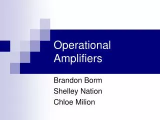
RF Amplifiers
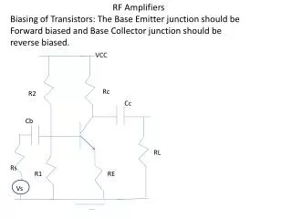
RF Amplifiers Biasing of Transistors: The Base Emitter junction should be Forward biased and Base Collector junction should be reverse biased. VCC. Rc. R2. Cc. Cb. RL. Rs. R1. RE. Vs. Equivalent Circuit:. Rs. gmvbe. Rc. Rl. RB. r p.

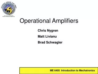
RF Amplifiers
E N D
Presentation Transcript
RF Amplifiers Biasing of Transistors: The Base Emitter junction should be Forward biased and Base Collector junction should be reverse biased. VCC Rc R2 Cc Cb RL Rs R1 RE Vs
Equivalent Circuit: Rs gmvbe Rc Rl RB rp Cp CL V Ccb Vs Small signal gain = gm (Rc II Rl)
Extending Bandwidth in RF Amplifiers Inductive load: L L C gmvbe R R C
Inductive load to enhance bandwidth Load impedance: Z(s) = (sL +R) II 1/sC = R[sL/R+1]/[S2 LC+ sRC + 1] If we define m=RC/[L/R], t = L/R Z(s) = R. [ts+ 1]/[s2t2m + stm +1] Gain with inductive load/gain wihoutindutcive load = |Z(jw)|/R = [ Band width with inductive load/Bandwidth without inductive load= Condition m=R2C/L Bandwidth boost factor Normalized Peak Freq.res Maximum bandwidth 1.41 1.85 1.19 |Z|=R 2 1.8 1.03 Best Magnitude Flatness 2.41 1.72 1 Beat delay flatness 3.1 1.6 1 No Shunt Peaking Infinite 1 1
10V Design Shunt Inductor Peaking amplifier 5nH CB1, coupling capacitor, Should offer Low resistance, les parasitics. 9k Rc=100 ohms Lm2 100pf Vout RB2, Bias resistor BFP193 1V Lm1 100pf .12V IE=10ma RL=50 ohms Rs= 50ohms RB1 1k RE=12 ohm. 1.5pF Vs Cm1 Current through bias resistors 10 times base current. Base current is =Emitter current/beta = 0.1mA.
Selection of Transistor BFP 193 RF transistor, ft, unity gain frequency = 8 GHz HFE = 125 (typical). All the transistor parameters have to be entered in the model. Package equivalent circuit. Package Equivalent Circuit: CCB= 19fF C B LBO= 0.65 nH LBI = 0.84 nH B Transistor Chip LCI = 0.07nH C LCO = 0.42nH E LEI = 0.31nH CCE=281fF CBE = 145fF LEO = 0.14 nH E
Design of Feedback Amplifier Let us design the amplifier for a power gain of 10 dB. This corresponds to a voltage gain of 3.2. 10 log Pout/Pin = 10 log Vout2/vin2 = 20 log Vout/Vin = 10db. Vout/Vin = (10) 0.5 = 3.3. Av= Vout/Vin = RC/RE=- 3.3 Rin =Rout =50 ohm. Rin = RF/ 1-Av = RF/1+3.3 RF = 50(4.3)= 215 ohm . You can select 210 ohm or 240 ohm as the RF. Select gm. Gain = gm. Ro= 3.3 = gm.50 gm = 3.3/50= 3300/50= 66 ms RE=1/gm= 1/ 66ms = 50/3.3= 15 ohm. Preferable value is about 12 ohm or 10 ohms. Gm=Ic/vt , Ic= 66.25= 1.5mA. We keep Ic about 10 mA so that we get enough gain. RL=500 ohms, so that VCB=5V to reduce Base to Collector capacitance.
10V CB1, reactance 10 times less than RB2 Rc=500 ohms to get adequate reverse bias to reduce Cbc RF, feedback resistor CB1, coupling capacitor, Should offer Low resistance, les parasitics. 3.3k .2k RB2, Bias resistor 5V BFP193 .9V .12V IE=10ma RL=50 ohms Rs= 50ohms RB1 1k RE=12 ohm. Vs Current through bias resistors 10 times base current. Base current is =Emitter current/beta = 0.1mA.
Matching Network At frequency wo, The impedance of the network = jwoLs+Rs =jwoLp|| Rp = = [(woLp)2Rp + jwoLpRp2]/Rp2+(woLp)2 Ls C Rs C Lp Rp Rp= Rs(Q2+1), Lp=Ls(Q2+1)/Q2 = Ls if Q>>1 Cp= Cs(Q2)/(Q2+1)
L match Circuit Ls Rp= Rs(Q 2 + 1) = RsQ 2 = Rs(1/(woRsC)2 = (1/Rs) (Ls/C) RsRp= Ls/C = Zo2 Rs Rp C Downward impedance transformer Ls Rp Rs C Upward impedance transformer
Tuned Amplifiers Gain x bandwidth = constant If we reduce the bandwidth, gain can be high. G (BW) = gmR.(1/RC) = gm/C
10V 5nH CB1, coupling capacitor, Should offer Low resistance, les parasitics. 9k Lm2 100pf Vout RB2, Bias resistor BFP193 1V Lm1 100pf .12V IE=10ma RL=50 ohms Rs= 50ohms RB1 1k RE=15 ohm. 1.5pF Vs Cm1 Current through bias resistors 10 times base current. Base current is =Emitter current/beta = 0.1mA.
Strange Impedance Behaviors and Stability Circuit Model for Base Impedance Effect: ib • The impedance seen at base of the transistor, • Zb= 1/jwCbe + Z(b+1) • = 1/jwCbe + Z(-jwT/w +1) • b = ic/ib = gm vbe/ib • = gm/sCbe =-j wT/w • goes to 1 at w =wT • 1 = gm/wT.Cbe, wT = gm/Cbe Cbe Zb bib Z If Z= R, resistor Zb sees it as a capacitor If Z is due to inductor, it appears as a resistance. If Z is a capacitor, it appears as –ve resistance and may cause oscillations.
Impedance Looking into the Emitter Terminal: Ze= 1/jwCbe + Z/(b+1) where Z is the impedance in the base side = 1/jwCbe + Z/ (-j wT/w +1) = 1/jwCbe + jZ(w/wT) If Z=jwL, Ze= = 1/jwCbe - (w2/wT) L Inductance at base appears as a negative resistance at emitter.