Nanometric thickness TiN sputtering coating for RF windows
410 likes | 797 Views
Nanometric thickness TiN sputtering coating for RF windows. E. Balsamo , M. Lacroix, A. Benardais, L.Grandsire, A. Frigo, and V. Palmieri, A. Variola. LNL,11 -10 - 2006. Outline: RF windows TiN characteristics and properties Methods : Reactive sputtering

Nanometric thickness TiN sputtering coating for RF windows
E N D
Presentation Transcript
Nanometric thickness TiN sputtering coating for RF windows E. Balsamo, M. Lacroix, A. Benardais, L.Grandsire, A. Frigo, and V. Palmieri, A. Variola LNL,11 -10 - 2006
Outline: • RF windows • TiN characteristics and properties • Methods : Reactive sputtering • TiN coating physical and chemical characterization
RF WINDOWS Pressure and Temperature transition and allow the RF power passage ceramic disk in alumina REMARK: ALUMINA • low rf loss and low outgassing rate • low rf loss and low outgassing rate • durable under heat treatment • resistant to the mechanical sollicitations • durable under heat treatment • resistant to the mechanical sollicitations H. Matsumoto
Breakdown of Al2O3 rf windows • Multipactor (1-100 MW):due to the high yield of secondary electron emission takes place during rf operation • Flash-over phenomena (30-250 MW):considered to be an avalanche of electrons which have been trapped in mechanically introduced defects. Breakdown and melting S. Michizono
A way for suppress multipactor • Coatingwith low SEE yield as Ti, Cr2O3,TiN on alumina. • BUT: • 1) very thin films could not sufficiently reduce SEE yield • 2) thick films cause excessive heating due to ohmic losses. • Optimize the thickness • ~10 nm
TITANIUM NITRIDE • conductive • chemically stable • hard material • USES: • cutting and grinding tools as a protective film • wear surfaces • decorative • - semiconductors and barrier layers • - superalloys to prevent whisker growth of Al2O3
TiN DEPOSITION TECNIQUES: • Vapor deposition in ammonia pressure; • Plasma Source Ion Implantation (PSII); • Thermochemical Nitridation; • High Velocity Oxygen Fuel Thermal Spray Process(HVOF); • Metal-Organic Chemical Vapor Deposition (MOCVD); • Atomic-Layer Chemical Vapor Deposition (ALCVD) using TiCl4 and NH3 as precursors; • by the reaction of titanium sol-gel with a nitrogenous admixture under laser irradiation; • Reactive Magnetron Sputtering (PVD).
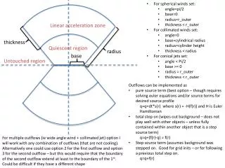
qt q0 Ar,N2 qc qp Pump θ1 1-θ1 target Area F F1 F2 F3 F4 ChamberArea θ2 1-θ2 J J F REACTIVE SPUTTERING: sputtering of an elemental target in presence of a gas, in our case N2. The reaction between the two partners will form a compound Target Stationary state during deposition Scheme of a reactive sputtering system Θ1= fraction target of compound molecules (1- θ1) = elemental non-reacted target atoms S.Berg
Deposition Deposition rate (a rate (a .u .u ) ) Hysteresis effect 1 1 Deposition rate (u.a) 0.8 0.8 Hysteresis region 0.6 0.6 0.4 0.4 0.2 0.2 1 1 2 2 3 3 4 4 Reactive Reactive gas gas flow flow ( ( sccm sccm ) ) Typical experimental curve for reactive sputtering process S.Berg
SCOPE: StoichiometricTiN film deposition with uniform fixed thickness on the whole surface (10 nm and 800nm) ON Al2O3 disk (Ø 50.8 mm, thickness 3.2 mm) Al2O3 cylinder (Ø 50 mm, height 60 mm) High purity of 99.7%
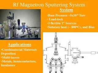
SPUTTERING CHAMBER 10” rotating magnetron Operating parameters for deposition of TiN Ti target (99,95 % purity) Working gas: Ar Reactive gas: N2
Method • Determine N2 and Ar partial pressure and distance target-substrate to obtain stoichiometric TiN; (on quarz 9 x 9 mm and sapphire 10 x 10) • Determine substrate position in order to obtain stoichiometric TiN on the whole surface; (on tempered glass 50 x 50 mm) • Good parameters control high reproducibility depositions • Determine deposition rate in such way to have the demanded thickness
Coating characterization PHYSICAL Film thickness: profilemeter Stoichiometry: XRD CHEMICAL Qualitative elementar analisy : SIMS Surface chemical analisy: ESCA
Stoichiometric TiN on quartzs (Distance target-substrate 134 mm and distance substrate respect target axis 105 mm) Increasing N2 pressure 8.0 ∙ 10-3 3.0 ∙ 10-3 8.0 ∙ 10-3 3.4 ∙ 10-3 Relationship between N2 partial pressureand deposition results of TiN. Film colour changes from metallic grey to gold , than brown with the increasing of nitrogen partial pressure.
TiN XRD Counts Sample 14 Position 2θ (degrees) Spectrum of diffracted X ray intensity versus 2θ angle
Diffractometry analysis in order to optimize the stoichiometry Counts Dark grey film Increasing N2 pressure UNDER STOICHIOMETRIC FILM
Diffractometry analysis in order to optimize the stoichiometry Counts Gold film Increasing N2 pressure UNDER STOCHIOMETRIC FILM Position 2θ (degrees)
Diffractomety analysis in order optimize the stoichiometry Counts Brown film STOICHIOMETRIC FILM!!!
Influence distance target-substrate to obtain stoichyometric TiN
Process parameters: = 3.4 ∙ 10 -3mbar = 8.0 ∙ 10 -3mbar Position disk: 4-8 cm from the centre of the target Deposition time: 10 nm ~ 12 sec 800 nm ~16 min and 46 sec In conclusion for planar sample: 9X9 mm TiN deposited quartz 45 mm ø alumina disk before deposition
DISK after deposition 10 nm 800 nm
Cylinder deposition Thickness variation vs distance from the target for vertical sample
25% from average 2 step deposition Cylinder deposition Percentual thickness variation vs distance from the target for vertical sample
CYLINDERafter deposition 10 nm 800 nm
12 nm Carbon : Pic C 1s Oxygèn : Pic O 1s Titanium : Pic Ti 2p3/2 Nitrogen : Pic N 1s ESCA RESULTS: • 1) Elementary and quantitative Analyses Within the limit of sensitivity of the technique (0.1 to 0.5% At.), no other element was detected (H and He nondetectable): 2) Chemical Formula of the detected elements The Ti / N stochiometric ratio is ~1 (error better than 2 %)
SIMS RESULTS • Ti : (46,47,48,49,50)Ti+, 96Ti2+ • N2 : 14N+, 26CN-, 62TiN+, 110Ti2N+, 124Ti2N2+ • C : 12C+, 12C-, 24C2- 26CN-, 38C2N-, 50C3N- 60TiC+, 74TiCN+, 108Ti2C+ • O2 : 16O+, 16O-, 42CNO-, 64TiO+, 64TiO-, 112Ti2O+, 126Ti2NO+
Conclusions: FROM ANALYSIS ESCA AND SIMS: TiN (+TixCy +Tix’Cy’Nz’ +Tix’’Oy’’Nz’’) CARBIDES, OXIDES, OXYNITRIDED AND CARBONITRIDES SUBSTRATE (alumina) TiN(1-x) with x ~ 0
Thanck you … for your attention
TiN DEPOSITION TECNIQUES: • HVOF; • PSII; • Thermochemical Nitridation; • Metal-Organic Chemical Vapor Deposition (MOCVD); • Atomic-Layer Chemical Vapor Deposition (ALCVD) using TiCl4 and NH3 as precursors; - considerably greater temperature range for deposition - • by the reaction of titania sol-gel with a nitrogenous admixture under laser irradiation; • Reactive Magnetron Sputtering (PVD).
PROFILOMETER Profilometer Alpha-Step 200
XRD The instrument
SIMS RESULTS principal detected elements: • Ti : (46,47,48,49,50)Ti+, 96Ti2+ • N2 : 14N+, 26CN-, 62TiN+, 110Ti2N+, 124Ti2N2+ • C : 12C+, 12C-, 24C2- 26CN-, 38C2N-, 50C3N- 60TiC+, 74TiCN+, 108Ti2C+ • O2 : 16O+, 16O-, 42CNO-, 64TiO+, 64TiO-, 112Ti2O+, 126Ti2NO+
XRD Counts Sample 14 Position (2 θ) Spectrum of diffracted X ray intensity versus 2θ angle