Download
1 / 19
190 likes | 366 Views
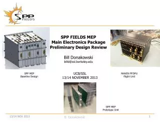
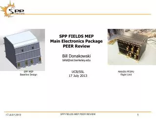
SPP FIELDS MEP Main Electronics Package PEER Review Bill Donakowski billd@ssl.berkeley.edu. UCB/SSL 17 July 2013. SPP MEP Baseline Design. MAVEN PFDPU Flight Unit. MEP Peer Review Overview. Requirements MAVEN Heritage Mechanical Overview Thermal Considerations

E N D
SPP FIELDS MEP Main Electronics Package PEER Review Bill Donakowski billd@ssl.berkeley.edu UCB/SSL 17 July 2013 SPP MEP Baseline Design MAVEN PFDPU Flight Unit
MEP Peer Review Overview Requirements MAVEN Heritage Mechanical Overview Thermal Considerations Dynamics Approach and Analysis Status and Schedule
MEP Requirements • Provide Packaging for 9 different Board Assemblies in common box • LNPS1, LNPS2, MAGo, MAGi, RFS/DCB, DFB, AEB (2x), TDS • Modular box arrangement that allows individual boxes to be built up independently and taken apart a/r • Design/Coordinate/Fab Box Frames with responsible groups • .060” thick Aluminum walls for Radiation Shielding • One plane mounting interface to Spacecraft • Adequate Structure Integrity (Strength, Dynamics) • Provide optimal thermal path to Spacecraft
MEP Challenges Provide common module for different boards Differing functions, connectors, and organizations (SSL/LASP/MN/GSFC) Box will be located in hot environment, must get heat out of box as much as possible (Thermal environment: baseline 75 C) Modular Frames must fit well together into final structural/thermal package Provide optimal thermal path to get heat out of boxes All frames must be in-plane for proper interface to Spacecraft Panel Mass is limited Column Grid Arrays require conformance to Steinberg / LASP requirements
MAVEN Design Heritage FIELDS MEP is modeled on MAVEN PFDPU Connectors on 3 sides of box Top EMI Shield over Card-Card Harnesses Box Vents (no shear panels) 10x Attach feet to S/C (every other Frame) S/C Bracket 6x Skewers 2x Skewers Box Size: 9.4” wide x 6.5” Tall x 8.0” long Box Size: 8.1” Wide x 6.2” Tall x 9.3” Long • SPP FIELDS Electronics Box • 9 Separate Cards sharing common Frame details • Bolted to S/C on one Box face • MAVEN Electronics Box • 11 Separate Cards sharing common Frame details • Bolted to S/C Bracket on one Box face
MEP Typ Box Frame Assy Intrabox Connectors Frame Instrument Connectors Spacecraft Connectors 6 x Skewers Screws and Custom Inserts at PCB perimeter Mounting Surface to Spacecraft
Box Machined Open Frame Box Frame walls .060” Multiple PCB attach screws to Frame to increase PWB stiffness and provide good thermal conduction path 6X Skewers (#8 Threaded Rod) Feet for attachment to S/C • Identical Open Frame Design for all Boxes except LNPS • LNPS to be 5-sided box • LNPSs mounted at stack ends Machined 6061 T6 Al Alloy Machined Frame .85” Pitch (Frame to Frame)
Upright Boxes bolted to S/C Bracket Individual Frames bolted together with 6X skewers Volume for Intrabox Cables Detail showing Frame Interlocking Features S/C Attach Surface
Card Assembly Overview Frame 6061 T6 EMI Shield Al Alloy, 1/32” Custom SSL threaded insert soldered to PCB (provided by SSL)
Daughter Board Details 4X Custom Tools Custom threaded tool thru threaded inserts applies gentle force at corners to remove DB from MB DB Module to be designed/built by SSL Large Chip (RJEX4000 CCGA) at Center Used on DCB, TDS, DFB
Connectors Fastening OTS Jackposts UCB Custom Connector Nutplate Blind hole to indicate Spiralock direction side of part D-Connector • Easier than nuts to assemble • no need to get wrench to hold nuts during jackpost torquing • Standoffs can be removed one-by-one Spiralock tapped holes APL desirement: allow changeout of connector jackposts w/o taking entire box apart late in the flow Solution: replace OTS nuts with custom nutplates Separate design for D-Connectors and MDM Connectors
MAVEN PFDPU Thermal Design S/C S/C PCB screwed to EMI Shield (2x) S/C S/C environment is hot—testing at 75 C Boards screwed to Frames (may be bonded if required) at perimeter 2X Screws at PCB center to EMI shield w/ integral posts Attachment frame wet mounted to S/C (TBC) Aluminum black anodized outside surfaces to radiate to S/C
Thermal Considerations: Center of PCB Screws at perimeter to frame Integral Posts at Center (fastened to PCB) EMI Shield with integral posts to PCB provide conductive path from center of PCB Shield screwed to Frames at perimeter
Thermal Modeling: Center Rib Tradeoff • Trade Study on Electronics Board performed • With Center Frame Rib • Without the Frame Rib • With integral standoff on EMI shield • Model: AEB Board, heat load of 1.17 W, 2 x 2 oz Cu Layers
PWB Thermal Design • Consider entire heat path • Component To Board • All components dissipating more than 50 mW should be looked at by thermal engineer • Thermal / Ground / Power Planes • Board dissipated power needs to travel to the frame via conduction in thermal (or ground) planes, then to the frame • Board Mounting to Box • Need a good path from thermal planes to standoffs / box lip / wedge locks etc
MEP FEM Dynamic Analysis • Requirements • Project: First Natural Frequency > 100 Hz • Steinberg Design: First Natural Frequency separation of 2X between individual PCB Assys and Entire Box
FEM Analysis: Preliminary Runs • PCB/Spacers/EMI Shield Assy • Fixed at Perimeters (to Frame) • Fn=195 Hz • Entire MEP Box Assy • (PCBs/Frames) • Fixed at Attach Feet (to S/C) • Fn > 600 Hz • Preliminary FEM Runs Encouraging • Fn > 100 Hz • Separation of 2X between PCB and Overall Structure • More detailed analysis required • With completed LNPSs design • Vibration testing of Prototype frames will confirm test results
MEP Status and Schedule • July 2013 • Baseline Design Completed • PCB sizing, connector locations, component heights, wall thicknesses, Frame details • PCB Layout ongoing at this time by responsible groups • LNPS work ongoing---not completed • FEM Analysis ongoing----first runs completed • August 2013 • Finish Frames design • Finish LNPS design • Complete FEM Analysis • Start Fab of Frames • September 2013 • Prototype Vibration Test of MEP Box • Verify Dynamics analysis • Finish thermal design • Finish Design Details • November 2013 • Instrument PDR