Single Cycle Processor Design
Learn about the step-by-step process of designing a processor, including datapath components, instruction execution control, and MIPS instruction formats. Review MIPS subset details and Register Transfer Level (RTL) descriptions.

Single Cycle Processor Design
E N D
Presentation Transcript
Single Cycle Processor Design COE 301 Computer Organization Prof. Aiman El-Maleh College of Computer Sciences and Engineering King Fahd University of Petroleum and Minerals [Adapted from slides of Dr. M. Mudawar, COE 301, KFUPM]
Presentation Outline • Designing a Processor: Step-by-Step • Datapath Components and Clocking • Assembling an Adequate Datapath • Controlling the Execution of Instructions • Main, ALU, and PC Control
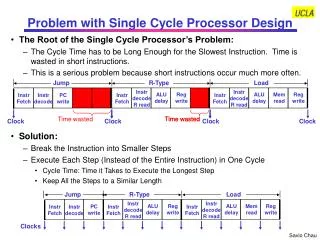
Designing a Processor: Step-by-Step • Analyze instruction set => datapath requirements • The meaning of each instruction is given by the register transfers • Datapath must include storage elements for ISA registers • Datapath must support each register transfer • Select datapath components and clocking methodology • Assemble datapath meeting the requirements • Analyze implementation of each instruction • Determine the setting of control signals for register transfer • Assemble the control logic
Review of MIPS Instruction Formats Op6 Rs5 Rt5 Rd5 sa5 funct6 Op6 Rs5 Rt5 immediate16 Op6 address26 • All instructions are 32-bit wide • Three instruction formats: R-type, I-type, and J-type • Op6: 6-bit opcode of the instruction • Rs5, Rt5, Rd5: 5-bit source and destination register numbers • sa5: 5-bit shift amount used by shift instructions • funct6: 6-bit function field for R-type instructions • immediate16: 16-bit immediate constant or PC-relative offset • address26: 26-bit target address of the jump instruction
MIPS Subset of Instructions • Only a subset of the MIPS instructions is considered • ALU instructions (R-type): add, sub, and, or, xor, slt • Immediate instructions (I-type): addi, slti, andi, ori, xori • Load and Store (I-type): lw, sw • Branch (I-type): beq, bne • Jump (J-type): j • This subset does not include all the integer instructions • But sufficient to illustrate design of datapath and control • Concepts used to implement the MIPS subset are used to construct a broad spectrum of computers
Register Transfer Level (RTL) • RTL is a description of data flow between registers • RTL gives a meaning to the instructions • All instructions are fetched from memory at address PC Instruction RTL Description ADDReg(rd) ← Reg(rs) + Reg(rt); PC ← PC + 4 SUBReg(rd) ← Reg(rs) – Reg(rt); PC ← PC + 4 ORIReg(rt) ← Reg(rs) | zero_ext(imm16); PC ← PC + 4 LWReg(rt) ← MEM[Reg(rs) + sign_ext(imm16)]; PC ← PC + 4 SW MEM[Reg(rs) + sign_ext(imm16)] ← Reg(rt); PC ← PC + 4 BEQ if (Reg(rs) == Reg(rt)) PC ← PC + 4 + 4 × sign_ext(offset16) else PC ← PC + 4
Instruction Fetch/Execute • R-typeFetch instruction: Instruction ← MEM[PC] Fetch operands: data1 ← Reg(rs), data2 ← Reg(rt) Execute operation: ALU_result ← func(data1, data2) Write ALU result: Reg(rd) ← ALU_result Next PC address: PC ← PC + 4 • I-type Fetch instruction: Instruction ← MEM[PC] Fetch operands: data1 ← Reg(rs), data2 ← Extend(imm16) Execute operation: ALU_result ← op(data1, data2) Write ALU result: Reg(rt) ← ALU_result Next PC address: PC ← PC + 4 • BEQ Fetch instruction: Instruction ← MEM[PC] Fetch operands: data1 ← Reg(rs), data2 ← Reg(rt) Equality: zero ← subtract(data1, data2) Branch: if (zero) PC ← PC + 4 + 4×sign_ext(offset16) else PC ← PC + 4
Instruction Fetch/Execute – cont’d concatenation • LWFetch instruction: Instruction ← MEM[PC] Fetch base register: base ← Reg(rs) Calculate address: address ← base + sign_extend(imm16) Read memory: data ← MEM[address] Write register Rt: Reg(rt) ← data Next PC address: PC ← PC + 4 • SW Fetch instruction: Instruction ← MEM[PC] Fetch registers: base ← Reg(rs), data ← Reg(rt) Calculate address: address ← base + sign_extend(imm16) Write memory: MEM[address] ← data Next PC address: PC ← PC + 4 • Jump Fetch instruction: Instruction ← MEM[PC] Target PC address: target ← PC[31:28] || address26 || ‘00’ Jump: PC ← target
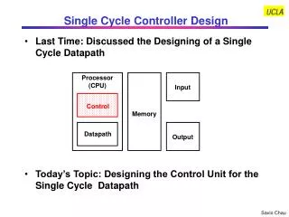
Requirements of the Instruction Set • Memory • Instruction memory where instructions are stored • Data memory where data is stored • Registers • 31 × 32-bit general purpose registers, R0 is always zero • Read source register Rs • Read source register Rt • Write destination register Rt or Rd • Program counter PC register and Adder to increment PC • Sign and Zero extender for immediate constant • ALU for executing instructions
Next . . . • Designing a Processor: Step-by-Step • Datapath Components and Clocking • Assembling an Adequate Datapath • Controlling the Execution of Instructions • Main, ALU, and PC Control
Components of the Datapath 32 zero A L U m u x 32 0 ALU result 16 32 Extend overflow 32 1 ExtOp ALUOp select 32 Instruction 32 32 PC 32 Address Instruction Memory • Combinational Elements • ALU, Adder • Immediate extender • Multiplexers • Storage Elements • Instruction memory • Data memory • PC register • Register file • Clocking methodology • Timing of writes Data Memory 32 Address 32 Data_out 32 Data_in clk clk clk Mem Read Mem Write Registers 5 32 BusA RA 5 32 RB BusB 5 RW BusW 32 RegWrite
Register Element Data_In n bits Register Write Enable Clock WE n bits Data_Out • Register • Similar to the D-type Flip-Flop • n-bit input and output • Write Enable (WE): • Enable / disable writing of register • Negated (0): Data_Out will not change • Asserted (1): Data_Out will become Data_In after clock edge • Edge triggered Clocking • Register output is modified at clock edge
MIPS Register File Register File 5 32 BusA RA 5 RB 32 5 BusB RW Clock BusW 32 RegWrite • Register File consists of 31 × 32-bit registers • BusA and BusB: 32-bit output busses for reading 2 registers • BusW: 32-bit input bus for writing a register when RegWrite is 1 • Two registers read and one written in a cycle • Registers are selected by: • RA selects register to be read on BusA • RB selects register to be read on BusB • RW selects the register to be written • Clock input • The clock input is usedONLY during write operation • During read, register file behaves as a combinational logic block • RA or RB valid => BusA or BusB valid after access time
Details of the Register File RA RB 5 5 Decoder Decoder 32 "0" "0" Tri-state buffers R1 WE R0 is not used 32 32 RW R2 WE . . . Decoder 32 5 . . . 32 32 32 BusW BusA R31 WE 32 RegWrite 32 BusB Clock
Tri-State Buffers Enable Data_in Data_out Data_0 Output Data_1 Select • Allow multiple sources to drive a single bus • Two Inputs: • Data_in • Enable (to enable output) • One Output: Data_out • If (Enable) Data_out = Data_in else Data_out = High Impedance state (output is disconnected) • Tri-state buffers can be used to build multiplexors
Building a Multifunction ALU 32 32 32 2 2 32 A d d e r ADD = 0 SUB = 1 Arithmetic Operation SLL = 00 SRL = 00 SRA = 01 ROR = 11 SLT: ALU does a SUB and check the sign and overflow 5 Shift/Rotate Operation Shift Amount Shifter 32 c0 0 ALU Result A sign ≠ 1 2 B 3 2 overflow zero ALU Selection Logic Unit 0 1 Shift = 00 SLT = 01 Arith = 10 Logic = 11 2 AND = 00 OR = 01 NOR = 10 XOR = 11 Logical Operation 3
Details of the Shifter • Implemented with multiplexers and wiring • Shift Operation can be: SLL, SRL, SRA, or ROR • Input Data is extended to 63 bits according to Shift Op • The 63 bits are shifted right according to S4S3S2S1S0 5 sa S4 S3 S2 S1 S0 SLL 16 8 4 2 1 0 0 0 0 0 split split split split split 31 31 31 31 31 63 47 39 35 33 32 32 16 31 16 8 31 8 4 31 4 2 31 2 1 31 1 Extender Data Data_out mux mux mux mux mux 31 31 31 31 31 1 1 1 1 1 16 8 4 2 1 2 Shift Right 0 or 1 bit Shift Right 0 or 2 bits Shift Right 0 or 4 bits Shift Right 0 or 8 bits Shift Right 0 or 16 bits Shift op
Details of the Shifter – cont’d • Input data is extended from 32 to 63 bits as follows: • If shift op = SRL then ext_data[62:0] = 031 || data[31:0] • If shift op = SRA then ext_data[62:0] = data[31]31 || data[31:0] • If shift op = ROR then ext_data[62:0] = data[30:0] || data[31:0] • If shift op = SLL then ext_data[62:0] = data[31:0] || 031 • For SRL, the 32-bit input data is zero-extended to 63 bits • For SRA, the 32-bit input data is sign-extended to 63 bits • For ROR, 31-bit extension = lower 31 bits of data • Then, shift right according to the shift amount • As the extended data is shifted right, the upper bits will be: 0 (SRL), sign-bit (SRA), or lower bits of data (ROR)
Implementing Shift Left Logical • The wiring of the above shifter dictates a right shift • However, we can convert a left shift into a right shift • For SLL, 31 zeros are appended to the right of data • To shift left by 0 is equivalent to shifting right by 31 • To shift left by 1 is equivalent to shifting right by 30 • To shift left by 31 is equivalent to shifting right by 0 • Therefore, for SLL use the 1’s complement of the shift amount • ROL is equivalent to ROR if we use (32 – rotate amount) • ROL by 10 bits is equivalent to ROR by (32–10) = 22 bits • Therefore, software can convert ROL to ROR
Instruction and Data Memories Data Memory 32 32 Data_out Address 32 Data_in 32 32 Clock Address Instruction Instruction Memory MemRead MemWrite • Instruction memory needs only provide read access • Because datapath does not write instructions • Behaves as combinational logic for read • Address selects Instruction after access time • Data Memory is used for load and store • MemRead: enables output on Data_out • Address selects the word to put on Data_out • MemWrite: enables writing of Data_in • Address selects the memory word to be written • The Clock synchronizes the write operation • Separate instruction and data memories • Later, we will replace them with caches
Clocking Methodology Combinational logic Register 2 Register 1 clock rising edge falling edge • Clocks are needed in a sequential logic to decide when a state element (register) should be updated • To ensure correctness, a clocking methodology defines when data can be written and read • We assume edge-triggered clocking • All state changes occur on the sameclock edge • Data must be valid and stable before arrival of clock edge • Edge-triggered clocking allows a register to be read and written during same clock cycle
Determining the Clock Cycle Combinational logic Register 1 Register 2 clock Tclk-q Tmax_comb Ts Th • With edge-triggered clocking, the clock cycle must be long enough to accommodate the path from one register through the combinational logic to another register • Tclk-q : clock to output delay through register • Tmax_comb: longest delay through combinational logic • Ts : setup time that input to a register must be stable before arrival of clock edge • Th: hold time that input to a register must hold after arrival of clock edge • Hold time (Th) is normally satisfied since Tclk-q > Th writing edge Tcycle ≥ Tclk-q + Tmax_comb + Ts
Clock Skew • Clock skew arises because the clock signal uses different paths with slightly different delays to reach state elements • Clock skew is the difference in absolute time between when two storage elements see a clock edge • With a clock skew, the clock cycle time is increased • Clock skew is reduced by balancing the clock delays Tcycle ≥ Tclk-q + Tmax_combinational + Tsetup+ Tskew
Next . . . • Designing a Processor: Step-by-Step • Datapath Components and Clocking • Assembling an Adequate Datapath • Controlling the Execution of Instructions • Main, ALU, and PC Control
Instruction Fetching Datapath next PC next PC 4 Improved Datapath A d d +1 32 32 30 30 32 32 00 Instruction Instruction 32 32 Address Address PC PC Instruction Memory Instruction Memory • We can now assemble the datapath from its components • For instruction fetching, we need … • Program Counter (PC) register • Instruction Memory • Adder for incrementing PC Improved datapath increments upper 30 bits of PC by 1 The least significant 2 bits of the PC are ‘00’ since PC is a multiple of 4 00 Datapath does not handle branch or jump instructions clk clk
Datapath for R-type Instructions RegWr ALUOp +1 30 Instruction Memory Registers 32 Rs 5 A L U 30 BusA RA 32 32 Instruction Rt 5 RB 32 Address BusB 32 Rd 5 RW ALU result BusW Op6 Rs5 Rt5 Rd5 sa5 funct6 00 PC • Control signals • ALUOpis the ALU operation as defined in the funct field for R-type • RegWr is used to enable the writing of the ALU result clk Rs and Rt fields select two registers to read. Rd field selects register to write BusA & BusB provide data input to ALU. ALU result is connected to BusW Same clock updates PC and Rd register
Datapath for I-type ALU Instructions RegWr ALUOp +1 30 Instruction Memory Registers 32 Rs 5 A L U 30 BusA RA 32 32 Instruction RB 32 Address BusB 32 Rt 5 RW ALU result BusW Extender ExtOp Imm16 00 Op6 Rs5 Rt5 immediate16 PC • Control signals • ALUOpis derived from the Op field for I-type instructions • RegWr is used to enable the writing of the ALU result • ExtOpis used to control the extension of the 16-bit immediate 5 32 Same clock edge updates PC and Rt clk Rt selects register to write, not Rd Second ALU input comes from the extended immediate. RB and BusB are not used
Combining R-type & I-type Datapaths RegWr +1 ALUOp 30 Instruction Memory Registers 32 Rs 5 A L U 30 BusA RA 32 32 Instruction Rt 32 5 RB 32 BusB Address 0 0 RW BusW 1 1 32 Rd ALUSrc ExtOp RegDst ALU result Extender Imm16 00 PC A mux selects RW as either Rt or Rd Another mux selects 2nd ALU input as either data on BusB or the extended immediate clk • Control signals • ALUOpis derived from either the Op or the funct field • RegWrenables the writing of the ALU result • ExtOpcontrols the extension of the 16-bit immediate • RegDst selects the register destination as either Rt or Rd • ALUSrcselects the 2nd ALU source as BusB or extended immediate
Controlling ALU Instructions RegWr= 1 +1 ALUOp 30 Instruction Memory Registers 32 Rs 5 A L U 30 BusA RA 32 32 Instruction Rt 32 5 RB 32 BusB Address RW 0 0 0 0 Rd BusW 1 1 1 1 ALUSrc = 0 ExtOp RegDst = 1 ALU result Extender Imm16 RegWr= 1 +1 ALUOp 30 Instruction Memory Registers 32 Rs 5 A L U 30 BusA RA 32 32 Instruction Rt 32 5 RB 32 00 00 BusB Address RW Rd BusW PC PC ExtOp RegDst = 0 ALUSrc = 1 ALU result 32 Extender Imm16 For R-type ALU instructions, RegDst is ‘1’ to select Rd on RW and ALUSrc is ‘0’ to select BusB as second ALU input. The active part of datapath is shown in green clk For I-type ALU instructions, RegDst is ‘0’ to select Rt on RW and ALUSrc is ‘1’ to select Extended immediate as second ALU input. The active part of datapath is shown in green clk
Details of the Extender Upper 16 bits . . . ExtOp Imm16 Lower 16 bits . . . • Two types of extensions • Zero-extension for unsigned constants • Sign-extension for signed constants • Control signal ExtOp indicates type of extension • Extender Implementation: wiring and one AND gate ExtOp = 0 Upper16 = 0 ExtOp = 1 Upper16 = sign bit
Adding Data Memory to Datapath ExtOp ALUOp MemRd MemWr 32 Imm16 ALUSrc WBdata ALU result +1 30 Instruction Memory Registers 32 Rs 5 Data Memory 0 0 0 BusA RA A L U 30 1 32 Instruction 1 Rt 5 Address RB 1 32 BusB Data_out Address Data_in RW Rd E BusW 32 32 RegDst Reg Wr 32 32 00 PC • A data memory is added for load and store instructions clk A 3rd mux selects data on BusW as either ALU result or memory data_out ALU calculates data memory address • Additional Control signals • MemRdfor load instructions • MemWrfor store instructions • WBdataselects data on BusW as ALU result or Memory Data_out BusB is connected to Data_in of Data Memory for store instructions
Controlling the Execution of Load MemRd = 1 MemWr = 0 WBdata = 1 Data Memory 0 0 0 1 1 Address 1 Data_out Data_in E 32 32 32 32 00 PC ALUOp = ADD ExtOp = 1 ALUSrc = 1 32 Imm16 ALU result +1 30 Instruction Memory Registers 32 Rs 5 BusA RA A L U 30 32 Instruction Rt 5 RB 32 BusB Address RW Rd BusW RegDst = 0 RegWr = 1 clk ExtOp = 1 to sign-extend Immmediate16 to 32 bits RegWr= ‘1’ to enable writing of register file RegDst = ‘0’ selects Rt as destination register ALUOp= ‘ADD’ to calculate data memory address as Reg(Rs) + sign-extend(Imm16) ALUSrc = ‘1’ selects extended immediate as second ALU input MemRd= ‘1’ to read data memory WBdata = ‘1’ places the data read from memory on BusW Clock edge updates PC and Register Rt
Controlling the Execution of Store MemRd = 0 MemWr = 1 WBdata = X Data Memory 0 0 0 1 1 Address 1 Data_out Data_in E 32 32 32 32 00 PC ALUOp = ADD ExtOp = 1 32 ALUSrc = 1 Imm16 ALU result +1 30 Instruction Memory Registers 32 Rs 5 BusA RA A L U 30 32 Instruction Rt 5 RB 32 BusB Address RW Rd BusW RegDst = X RegWr = 0 clk ExtOp = 1 to sign-extend Immmediate16 to 32 bits RegWr= ‘0’ to disable writing of register file RegDst = ‘X’ because no register is written ALUOp= ‘ADD’ to calculate data memory address as Reg(Rs) + sign-extend(Imm16) ALUSrc = ‘1’ selects extended immediate as second ALU input MemWr= ‘1’ to write data memory WBdata = ‘X’ because don’t care what data is put on BusW Clock edge updates PC and Data Memory
Adding Jump and Branch to Datapath 1 0 0 1 PCSrc Adding a mux at the PC input ExtOp Branch Target Address 2 Jump Target = PC[31:28] ‖ Imm26 New adder for computing branch target address 1 0 Next PC Address + E Imm16 +1 ALU result Rs Rt Zero 0 Rd 1 Reg Dst Instruction Memory Registers Data Memory RegWr BusA ALU Op Mem Wr WB data Mem Rd RA A L U 00 ALU Src clk Address Address RB PC Op Data_out Instruction BusB Data_in RW BusW • Additional Control Signals • PCSrcfor PC control: 1for a jump and 2 for a taken branch • Zero flag for branch control: whether branch is taken or not
Controlling the Execution of a Jump 1 0 0 1 PCSrc = 1 ExtOp = X Branch Target Address If (Opcode == J) then PCSrc = 1 (Jump Target) 2 Jump Target = PC[31:28] ‖ Imm26 1 0 Next PC Address + E Imm16 +1 ALU result Rs Rt Zero = X 0 Rd 1 Reg Dst = X Instruction Memory Registers Data Memory Reg Wr = 0 BusA ALU Op = X Mem Wr = 0 WB data = X Mem Rd = 0 RA A L U 00 ALU Src = X clk Address Address RB PC Op = J Data_out Instruction BusB Data_in RW BusW MemRd = MemWr = RegWr = 0, Don't care about other control signals Clock edge updates PC register only
Controlling the Execution of a Branch 1 0 0 1 PCSrc = 2 ExtOp = 1 If (Opcode == BEQ && Zero == 1) then PCSrc = 2 (Branch Target) else PCSrc = 0 (Next PC) Branch Target Address 2 Jump Target = PC[31:28] ‖ Imm26 1 0 Next PC Address + E Imm16 +1 ALU result Rs Rt Zero = 1 0 Rd 1 Reg Dst = X Instruction Memory Registers Data Memory Reg Wr = 0 BusA ALU Op = SUB Mem Wr = 0 WB data = X Mem Rd = 0 RA A L U 00 ALU Src = 0 clk Address Address RB PC Op BEQ Data_out Instruction BusB Data_in RW BusW ALUSrc = 0, ALUOp = SUB, ExtOp = 1, MemRd = MemWr = RegWr = 0 Clock edge updates PC register only
Next . . . • Designing a Processor: Step-by-Step • Datapath Components and Clocking • Assembling an Adequate Datapath • Controlling the Execution of Instructions • Main, ALU, and PC Control
Main, ALU, and PC Control ALU Control Main Control Input • 6-bit opcode field Main Control Output • Main control signals Zero Instruction Memory Datapath A L U Address PC 32 Instruction WBdata MemWr MemRd RegDst RegWr ExtOp ALUSrc Op6 ALUOp PCSrc 0 funct6 PC Control Zero Main Control 1 2 Op6 ALU Control Input • 6-bit opcodefield • 6-bit functionfield ALU Control Output • ALUOpsignal for ALU PC Control Input • 6-bit opcode • ALU zero flag PC Control Output • PCSrc signal
Single-Cycle Datapath + Control 1 0 0 1 MemRd WBdata Main Control RegDst RegWr MemWr ExtOp ALUSrc PC Ctrl ALU Ctrl ExtOp Branch Target Address 0 Jump Target = PC[31:28] ‖ Imm26 1 Next PC Address 2 + Ext Imm16 +1 ALU result Rs Rt 0 PCSrc Rd Zero 1 Instruction Memory Registers Data Memory BusA ALUop RA A L U 00 clk func Address Address RB PC Data_out Instruction BusB Op Data_in RW BusW Zero
Main Control Truth Table X is a don’t care (can be 0 or 1), used to minimize logic
Logic Equations for Main Control Signals SLTI R-type ADDI ANDI ORI XORI LW SW RegDst = R-type RegWrite = (SW + BEQ + BNE + J) ExtOp = (ANDI + ORI + XORI) ALUSrc = (R-type + BEQ + BNE) MemRd = LW MemWr = SW WBdata = LW Op6 Decoder BEQ BNE J Logic Equations RegDst RegWr ExtOp ALUSrc MemRd WBdata MemWr
ALU Control Truth Table The 4-bit Coding defines the binary ALU operations. Logic equations are derived for the 4-bit coding. Other bit-coding can be used. The goal is to simplify the ALU control.
PC Control Truth Table The ALU Zero flag is used by BEQ and BNE instructions
PC Control Logic • The PC control logic can be described as follows: if (Op == J) PCSrc = 1; else if ((Op == BEQ && Zero == 1) || (Op == BNE && Zero == 0)) PCSrc = 2; else PCSrc = 0; Op Decoder Branch = (BEQ.Zero) + (BNE.Zero) Branch = 1, Jump = 0 PCSrc = 2 Branch = 0, Jump = 1 PCSrc = 1 Branch = 0, Jump = 0 PCSrc = 0 BEQ BNE J Zero Branch Jump
Worst Case Timing (Load Instruction) Clk Clk-to-q Old PC New PC Instruction Memory Access Time Old Instruction New Instruction = (Op, Rs, Rt, Rd, Funct, Imm16, Imm26) Delay Through Control Logic Old Control Signal Values New Control Signal Values (ExtOp, ALUSrc, ALUOp, …) Register File Access Time Old BusA Value New BusA Value = Register(Rs) Delay Through Extender and ALU Mux Old Second ALU Input New Second ALU Input = sign-extend(Imm16) ALU Delay New ALU Result = Address Old ALU Result Data Memory Access Time Old Data Memory Output Value New Value Mux delay + Setup time + Clock skew Write Occurs Clock Cycle
Worst Case Timing – Cont'd • Long cycle time: must be long enough for Load operation PC’s Clk-to-Q + Instruction Memory’s Access Time + Maximum of ( Register File’s Access Time, Delay through control logic + extender + ALU mux) + ALU to Perform a 32-bit Add + Data Memory Access Time + Delay through MemtoReg Mux + Setup Time for Register File Write + Clock Skew • Cycle time is longer than needed for other instructions
Summary • 5 steps to design a processor • Analyze instruction set => datapath requirements • Select datapath components & establish clocking methodology • Assemble datapath meeting the requirements • Analyze implementation of each instruction to determine control signals • Assemble the control logic • MIPS makes Control easier • Instructions are of the same size • Source registers always in the same place • Immediate constants are of same size and same location • Operations are always on registers/immediates