Single-Cycle Processor Design
Single-Cycle Processor Design. CS 3220 Fall 2014 Hadi Esmaeilzadeh hadi@cc.gatech.edu Georgia Institute of Technology Some slides adopted from Prof. Milos Prvulovic. Single-Cycle Approach. Entire instruction done in only one cycle Data-moving takes only time it really needs (wires)

Single-Cycle Processor Design
E N D
Presentation Transcript
Single-Cycle Processor Design CS 3220 Fall 2014 Hadi Esmaeilzadeh hadi@cc.gatech.edu Georgia Institute of Technology Some slides adopted from Prof. Milos Prvulovic
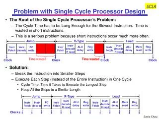
Single-Cycle Approach • Entire instruction done in only one cycle • Data-moving takes only time it really needs (wires) • E.g. dedicated wire to take reg output to ALU input • Control takes only as much time as it really needs • Figure out all control signals right after inst read from imem • Takes only part of one cycle, because one is all we have • All major units get used in every cycle • Unless the unit is not needed for a specific instruction • But…“enhancements” become “necessities” • Example: Branch uses ALU to compare, need separate PC+4+4*imm • Each cycle, need to read two registers read and writte one • Etc. • And… longest-to-do instruction determines clock • Usually a load, so all other insts will have slack for memory read
Single-cycle Supported: ADD + 4 Control P C Instr Mem RF
Look at that register file! module RegFile(RADDR1,DOUT1,RADDR2,DOUT2,WADDR,DIN,WE,CLK); parameter DBITS; // Number of data bits parameter ABITS; // Number of address bits parameter WORDS = (1<<ABITS); parameter MFILE = ""; reg [(DBITS-1):0] mem[(WORDS-1):0]; input [(ABITS-1):0] RADDR1,RADDR2,WADDR; input [(DBITS-1):0] DIN; output wire [(DBITS-1):0] DOUT1,DOUT2; input CLK,WE; always @(posedge CLK) if(WE) mem[WADDR]=DIN; assign DOUT1=mem[RADDR1]; assign DOUT2=mem[RADDR2]; endmodule • Three separate accesses • Two reads • One write • Each with it own address!
Wire it up wire [3:0] rregno1=rs, rregno2=rt; wire [(DBITS-1):0] regout1,regout2; wire [3:0] wregno=rd; // This comes from decoding logic // (reg becomes wire in non-edge always block) regwrreg; reg [(DBITS-1):0] wregval; // Now instantiate the register file module RegFile #(.DBITS(DBITS),.ABITS(5), regFile( .RADDR1(rregno1),.DOUT1(regout1), .RADDR2(rregno2),.DOUT2(regout2), .WADDR(wregno), .DIN(wregval), .WE(wrreg),.CLK(clk));
Wire it up - ALU // ALU input 1 is always the first source register wire [(DBITS-1):0] aluin1=regout1; // ALU input 2 is decided by control logic // (either regout2 or immediate) reg [(DBITS-1):0] aluin2; // Decided by control logic reg[4:0] alufunc; // Output of the ALU (becomes wire b/c of always block below) reg[(DBITS-1):0] aluout; always @(alufuncor aluin1 or aluin2) case(alufunc) OP2_AND: aluout=aluin1&aluin2; ... // Same as in Project 2 ... // but uses aluin1 and aluin2 instead of A and B // Used by control logic for conditional branches wire cond=aluout[0];
Control Logic always @(opcode1 or opcode2 or ry or rz) begin {aluimm,alufunc,isbranch,isjump,wrmem}= { 1'bX, 5'hXX, 1'b0, 1'b0, 1'b0}; {selaluout,selmemout,selpcplus,wrreg}= { 1'bX, 1'bX, 1'bX, 1'b0}; case(opcode1) OP1_ALUR: {aluimm, alufunc, selaluout,selmemout,selpcplus,wrreg}= { 1'b0,{1’b0,op2_i}, 1'b1, 1'b0, 1'b0, 1'b1}; OP1_ALUI: {aluimm, alufunc, selaluout,selmemout,selpcplus,wrreg}= { 1'b1,{1’b0,op2_t}, 1'b1, 1'b0, 1'b0, 1'b1}; …
Single-cycle Supported: ADD, ADDI 4 Control P C Instr Mem RF M X SE
Single-cycle Supported: All ALUR,ALUI insts 4 Control P C Instr Mem RF M X SE
Single-cycle Supported: ALUR, ALUILW 4 Control P C Instr Mem RF Data Mem A M X M X SE
Single-cycle Supported: ALUR, ALUILW, SW Control 4 P C Instr Mem RF A Data Mem M X M X D SE
Single-cycle Supported: ALUR, ALUI LW, SW BCOND M X aluout[0] Control 4 P C Instr Mem RF A Data Mem M X M X D SE
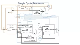
And it’s not done yet! Supported: ALUR, ALUI,LW, SW,BCOND JAL M X Control 4 P C Instr Mem RF A Data Mem M X M X D SE
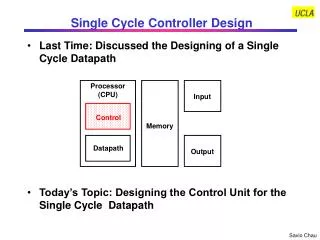
How do we do all this? • The only real “state” is the PC, Regs, and Mem • The rest is just wires and combinatorial logic • Central control takes opcode,generates all signals for the entire instruction! • But can have other small pieces of control • E.g. decide if PC+4 or PC+4+Offs loadedinto PC on a conditional branch instruction, or to load a register for the JAL instruction