Single Cycle Controller Design
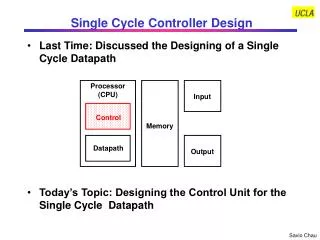
Single Cycle Controller Design. Last Time: Discussed the Designing of a Single Cycle Datapath. Processor (CPU). Input. Control. Memory. Datapath. Output. Today’s Topic: Designing the Control Unit for the Single Cycle Datapath. Steps to Design a Processor. 5 steps to design a processor

Single Cycle Controller Design
E N D
Presentation Transcript
Single Cycle Controller Design • Last Time: Discussed the Designing of a Single Cycle Datapath Processor (CPU) Input Control Memory Datapath Output • Today’s Topic: Designing the Control Unit for the Single Cycle Datapath
Steps to Design a Processor • 5 steps to design a processor • 1. Analyze instruction set => datapath requirements • Define the instruction set to be implemented • Specify the implementation requirements for the datapath • Specify the physical implementation • 2. Select set of datapath components & establish clock methodology • 3. Assemble datapath meeting the requirements • 4. Analyze implementation of each instruction to determine setting of control points that effects the register transfer. • 5. Assemble the control logic • MIPS makes it easier • Instructions same size • Source registers always in same place • Immediates same size, location • Operations always on registers/immediates Datapath Design Cpntrol Logic Design See Example
Step 4: Determine Control Points of the Data PathGeneral Ideas • Where to find the control points? Common Places are: • Read / Write Enable Signals for State Elements (Memory, Register File) • Enable Signals for Combinational Logic (e.g., SignExtender) • Control Signals that Determine ALU Operations • Select Signals for Multiplexors • Control Signals in Any Data Path Components • How to Determine the Setting of the Control Signals • Need to Understand the Operations of the Components in Different Control Signal Setting • Need to Understand How the Data is Supposed to Flow Through the Data Path for Each Instruction
Step 4: Determine Control Points of the Data Path Control Signal for Instruction Fetch • Fetch the Instruction from Instruction Memory: Instruction mem[ PC] • For single cycle data paths, there is no control signal for the PC because it is updated every clock. This is true for all instructions
Step 4: Determine Control Points of the Datapath Control Signals for Add Instruction • R[ rd] R[ rs] + R[ rt] Branch = 0 Jump = 0 RegDst = ? RegDst = 1 ALUctr = ? ALUctr ALUctr = add RegWr = ? RegWr = 1 MemtoReg = ? MemtoReg = 0 MemWr = 0 ExtOP = x ALUSrc = ? ALUSrc = 0
Step 4: Determine Control Points of the Datapath Control Signals for Or Immediate • R[ rt] R[ rs] or ZeroExt( imm16) Branch = 0 Jump = 0 RegDst = 0 RegDst = ? ALUctr = ? ALUctr = or ALUctr RegWr = 1 RegWr = ? MemtoReg = 0 MemtoReg = ? MemWr = 0 ExtOP = ? ExtOP = 0 ALUSrc = ? ALUSrc = 1
Step 4: Determine Control Points of the Datapath Control Signals for Load • R[ rt] Data Memory [R[ rs] + SignExt( imm16)] Branch = 0 Jump = 0 RegDst = 0 RegDst = ? ALUctr = add ALUctr = ? ALUctr RegWr = 1 RegWr = ? MemtoReg = 1 MemtoReg = ? MemWr = 0 ExtOP = 1 ExtOP = ? ALUSrc = ? ALUSrc = 1
Step 4: Determine Control Points of the Datapath Control Signals for Store • Data Memory [R[rs] + SignExt(imm16) ] R[rt] Branch = 0 Jump = 0 RegDst = x ALUctr = add ALUctr = ? ALUctr RegWr = 0 MemtoReg = x MemWr = 1 MemWr = ? R[rt] ExtOP = 1 ExtOP = ? ALUSrc = ? ALUSrc = 1
Instruction Fetch Unit at the End of Instructions Except for Branch and Jump • PC PC + 4 • This is the Same for all Instructions Except: Branch and Jump Jump = 0 Branch = 0 Zero = x ExtOP = x
Step 4: Determine Control Points of the Datapath Control Signals for Branch • If (R[rs] - R[rt] == 0 ) Then Zero 1 ; else Zero 0 Branch = ? Jump = ? RegDst = x ALUctr ALUctr = ? ALUctr = sub Zero See next page RegWr = 0 MemtoReg = x MemWr = 0 ExtOP = x ALUSrc = ? ALUSrc = 0
Instruction Fetch Unit at the End of Branch • If ( Zero == 1 ) Then PC = PC + 4 + SignExt( imm16) * 4 ; Else PC = PC + 4 Jump = 0 Branch = 1 Zero = 1 ExtOP = 1
Step 4: Determine Control Points of the Datapath Control Signals for Jump • The data path has nothing to do! Make sure control signals are set correctly!
Instruction Fetch Unit at the End of Jump • PC PC_incr< 31: 28> concat target< 25: 0> concat “00” Jump = 1 Branch = 0 Zero = x ExtOP = X
Step 4: Determine Control Points of the Datapath All Required Control Signals for the Given Data Path Instruction<31:0> Instruction Memory <0:15> <21:25> <21:25> <16:20> <11:15> Adr Op Fun Rt Rs Rd Imm16 Control Branch Jump RegWr RegDst ExtOp ALUSrc ALUctr MemWr MemtoReg Zero DATA PATH
For single cycle data path, this is just a big decoder! 0 1 1 1 1 + lw Control Unit 1 1 X 0 0 + add Op Code Step 5: Assemble the Control Logic Example: Control signals for a combined data path for add and lw instructions Questions: (1) How to make sure the control signals have correct values for different instructions? Ans: Need a control unit to generate control signals for instructions (2) How does the control unit look like? Next Addr Logic PC+4 PC ALUctr RegWr ExtOP ALUsrc RegDst MemtoReg Instruction Memory rs R[rs] RA1 Data Memory Register File rt RA2 ALU 0 rd mux WA R[rt] 1 imm16 mux Wr data 0 1 ext 0 mux 1 See Control Unit Design Example
Step 5: Assemble the Control LogicControl Signals for a Full Control Unit These signals can easily be expressed as functions of the opcodes See following discussions
See next slide With local decoding, Main Control has only 26 = 64 minterms and local control has only 29 = 512 minterms The Concept of Local Decoding 6 func Without local decoding, Main Control has to include func input and will have 26+6 = 4K minterms
Encoding ALUop Address concatenation do not need ALU I-type op For R-type, actual operation is determined by the func field (see text p. 153 for func encoding) Add offset to address for lw and sw Subtract to compare
Truth Table for ALUctr op I-type uses the opcodes but not the func field R-type has only 1 opcode but uses the func field for encoding • ALUop = f (opcode) ; as shown in the previous slide • ALUctr = f (ALUop, func)
op[1:0] Binvert Binvert op[1:0] cin a0 a 0 result0 b0 0 0 1 1 1 sum + result b 2 a1 result1 b1 Less sum 3 cin 0 cout a b op[1:0] Binvert cout Cin Cin ALU1 ALU0 cin zero a 0 Less Less Cout Cout Cin 1 ALU31 a31 result31 b31 overflow sum + Less result b 0 2 set Less 3 set overflow Overflow detection ALUctr Signals
Logic Equations for the ALUctr Signals This makes func< 3> a don’t care ALUctr<2>: ALUctr<2> = !ALUop<2> & !ALUop<1> & ALUop<0> + ALUop<2> & !ALUop<1> & !ALUop<0> & !func<2> & func<1> & ! func<0> ALUctr<1>: ALUctr<1> = !ALUop<2> & !ALUop<1> + ALUop<2> & !ALUop<1> & !ALUop<0> & !func< 2> ALUctr<0>: ALUctr<0> = !ALUop<2> & ALUop<1> & !ALUop< 0>+ ALUop<2> & !ALUop<1> & !ALUop<0> & !func<3> & func<2> & !func<1> & func<0>+ ALUop<2> & !ALUop<1> & !ALUop<0> & func<3> & !func< 2> & func< 1> & ! func< 0>
The “Truth Table” for the Main Control See last 4 slides
Implementation of the Main Control UnitExample: the RegWrite Control Signal RegWrite = R- type + ori + lw = !op<5> & !op<4> & !op<3> & !op<2> & !op<1> & !op<0> (i.e., R- type) + !op<5> & !op<4> & op<3> & op<2> & !op<1> & op<0> (i.e., ori) + op<5> & !op<4> & !op<3> & ! op<2> & op<1> & op<0> (i.e., lw) Key Idea: Any controller output signal can be expressed as a logical sum (i.e., or) of logical products (i.e., and terms)
Step 5: Assemble the Control Logic (Summary) Implementation of the Entire Main Control
clock clock Putting It All Together: A Single Cycle Processor clock
Single Cycle ProcessorDelay Path Comparisons for Three Instruction Types Clock (T1) 1 Clock Cycle Clock (T2)
Worst Case Timing: Load Instruction Clk to-Q Old Value New Value Instruction Memory Access Time Old Value New Value Delay Through Control Logic Old Value New Value Old Value New Value Old Value New Value RegWr busA busB Address busW Old Value New Value Register File Access Time Old Value New Value Delay through Extender & Mux Old Value New Value ALU Delay Old Value New Value Data Memory Access & MUX Time Old Value New Value
Drawback of the Single Cycle Processor • Long Cycle Time: • Cycle Time Must be Long Enough for the Load Instruction= + PC’s Clock- to- Q + Instruction Memory Access Time + Register File Access Time + ALU Delay (address calculation) + Data Memory Access Time + Register File Setup Time • Cycle Time is Much Longer than Needed for all Other Instructions