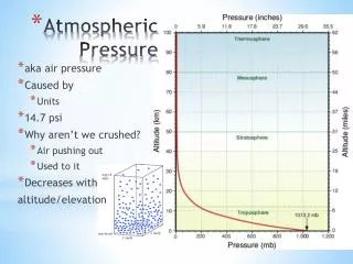
Download
1 / 10
110 likes | 297 Views
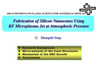
18th SYMPOSIUM ON PLASMA SCIENCE FOR MATERIALS (SPSM-18). Fabrication of Silicon Nanocones Using RF Microplasma Jet at Atmospheric Pressure. ○. Zhongshi Yang. Research Background Micro-analysis of the Cone Structures Mechanism of the SNC Growth Conclusions. 背景.

E N D
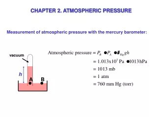
18th SYMPOSIUM ON PLASMA SCIENCE FOR MATERIALS (SPSM-18) Fabrication of Silicon Nanocones Using RF Microplasma Jet at Atmospheric Pressure ○ Zhongshi Yang • Research Background • Micro-analysis of the Cone Structures • Mechanism of the SNC Growth • Conclusions
背景 Research Background Synthesis of silicon and carbon nanostructures CNTsNanocones Nanopillars field emission devices, UV laser, FET, sensors CVD, laser ablation, RIE, electrodeposition RF microplasma jet at atmospheric pressure on Fe coated c-Si using a CH4-Ar mixture
Atmospheric RF Microplasma Jet ArPlasma CH4 Fe c-Si • Fabrication Conditions • Cathode:WCtube with d of 700 µm • Substrate: Fecoated c-Si • Fr(Ar):50sccm Fr(CH4) :50 sccm • D : 4 mm Ts:400ºC RF power:40W
Surface distribution underneath the tube electrode The inner diameter of Electrode : 700 µm : 400μm A SEMImage C C : 600 800 m : 400 600 m : 600 m : 400 600 m ~ μ ~ μ B ~ μ ~ μ B 1.5μm 100nm 100nm
5μm 5μm Fe C 5μm 5μm composition distribution of the cones Surface Distribution of elements SEMImage O Si 5μm EDX Spectra Come-shaped products were mainly composed of silicon and SiO2. Siliconnanocones (SNCs)
TEM像 Si Si 1 μ m 1 μ m 1 μ m 1 μ m TEM for SNC and CNT B region Aregion SNC CNT 67nm 14nm 60 nm EDX analysis SNWs 20nm Si nanocrystals are embedded in the cone region
Growth Condition of Si Nanocones plasma substrate results (a) Ar & Ar+CH4 plasma c-Si etched hole& no cones (b) Arplasma Fe/c-Sietched hole& no cones (c) Ar+CH4 plasma Fe/c-Si SNCs, SNWs, CNTs Linear Surface Profile Fe/c-Si surface CH4 introduction and Fe film are very important to the SNCs growth.
② 照射時間依存 SNCs Formation (as a function of exposure time) 1min 10min H R 1μm 1μm 30min 60min ・Number density increased ・Average size increased 1μm 1μm
Growth Model of SNCs Tg: 2000~3000K Ar plasma jet CH4 CH4 ~20 nm thick Fe layer Si oxidation nc-Si particle c-Si 1Highgas temperature(2000-3000K)of Armicroplasma jet. 2Formation of FeSix and FeCx nanoclusters. 3 Catalytic growth by a diffusion of Si and nanocrystalline silicon particles through the FeSix nanoclusters. 4Silicon oxidation at the outer walls by the plasma heating.
18th SYMPOSIUM ON PLASMA SCIENCE FOR MATERIALS (SPSM-18) Conclusions • Si Nanocones (SNCs) were synthesized on Fe-coated c-Si using RFmicroplasma jet at atmospheric pressure. Thanks for your attention !