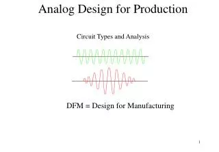
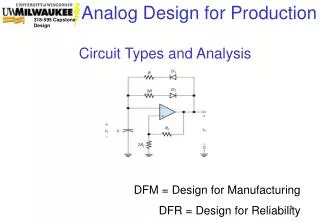
Circuit Types and Analysis
Circuit Types and Analysis. DFM = Design for Manufacturing DFR = Design for Reliability. Linear Analog Circuit Blocks. Amplifiers and Attenuators Math Functions (add, subtract) Oscillators (sinusoidal) Filters Voltage Regulators Voltage References. Non-Linear Analog Circuit Blocks.

Circuit Types and Analysis
E N D
Presentation Transcript
Circuit Types and Analysis • DFM = Design for Manufacturing • DFR = Design for Reliability
Linear Analog Circuit Blocks • Amplifiers and Attenuators • Math Functions (add, subtract) • Oscillators (sinusoidal) • Filters • Voltage Regulators • Voltage References
Non-Linear Analog Circuit Blocks • Comparators • Oscillators (non-sinusoidal, square, sawtooth, etc) • Voltage Limiters and Clamps • Rectifiers and Bridges • Math Functions (multiply, divide) • Log and other Non-linear Amplifiers • Sample and Hold Amplifiers • Envelope & Peak Detectors • Phase Detectors • Phased Locked Loops • Switching Voltage Regulators
Passive Components, R-L-C • Critical Factors: • Ambient Temperature • Thermal Deratings & Variation of Primary Parameter (Temp Co) • Maximum Imposed Voltage and/or Current • Maximum Imposed dV/dT and/or Frequency • Inductive Frequency (high frequency model) • Minimum Analysis & Selection Considerations: • Primary Parameter Tolerances (R, L, C %) • Total Power vs Package Dissipation • Maximum Voltage • Composition, Specific die-electrics, construction, etc
Passive Discretes • Resistors/Inductors: Must specify or account for Tolerance, Power, Package and Temp Coefficient • Derating Guide: ~50% of rated power or current • Std Tolerances: 0.1%, 1%, 5%, 10% and 20% • Constructional Anomalies: Max Voltage, Inductive with High Freq • Capacitors: Must specify or account for Tolerance, WV, Polarization, Dielectric, Temp Co and Package • Derating Guide: ~50% of rated voltage • Std Tolerances: 1%, 2%, 5%, 10%, 20%, 80% • Constructional Anomalies: Charge Leakage, Inductive with High Freq,
+ - • Amplifiers
Small Signal Amplifiers • Critical Factors: • Component Tolerances, particularly gain setting R’s • OpAmp Input Offset Voltage (Vio), worse for high gain • Input Bias Current (Ib), Input Offset Current (Iio) • Finite Diff Gain (Ad) & Variation of Ad with Frequency • Output Slew Rate and Output Vp-p at Maximum Frequency • Worst Case Analysis: • Total DC Offset error in Volts (1,2,3) • Total Gain Error vs Nominal, Converted to Volts (1,4) • Power Bandwidth for Application (1,5)
Basic Gain in Voltage, Current or CombinationLinear Operation: No New Frequencies Created • Voltage Amplifiers (Vin >> Vout): Av = Vout/Vin • Current Amplifiers (Iin >> Iout): Ai = Iout/Iin • Transimpedance (Iin >> Vout): Zm = Vout/Iin • Transconductance (Vin >> Iout): Gm = Iout/Vin Additional Parameters • Input Impedance: Zin = Vin/Iin • Output Impedance: Zout = {Vout(NL) – Vout(L)}/Iout • Slew Rate (SR): Min dVout/dT • Slew Rate BW = SR/2pVp where Vp = Peak Voltage
+ - Operational AmplifierLinear, Differential, High Gain Amplifier Advantages Over Single Ended Amplifier Block ?? • Easy to add positive and negative feedback with differential input • Single Ended Application Gains can be tightly controlled with external components and made insensitive to internal transistor gain variations • Inherent noise rejection when noise enters both input terminals
+ - Operational AmplifierIdeal Assumptions Vp Used for basic analysis, nominal gain analysis Vout • Vout = Ad (Vp – Vn) where Ad is the diff gain • Ad = Infinite • Zin = Infinite, Iin = 0 where Iin is the input current • Vp = Vn because of infinite Ad, Vo may be non-zero under this condition • Iout = Infinite (Often a false assumption) These basic assumptions allow simple circuit analysis to determine Nominal gain applications Vn
+ - Operational AmplifierPower Supplies Vcc Vp Power Supplies can be a critical consideration Vout • -Vcc < Vout < Vcc At all times, Vout(max) may be as low as 2 to 5 volts below Vcc depending upon model • Vcc, -Vcc sometimes referred to as “Rails” due to power distribution on some boards resembling tracks • Many applications use “Split” supply Operation • Split Supply means Vcc = |-Vcc| • Some models characterized for 1 supply operation (but ALL will work there) • Single Supply means –Vcc = 0 • Vcc, -Vcc power pins should always be capacitively filtered with 0.1uf (usually ceramic monolithic X7R or similar) Vn -Vcc
+ - Operational AmplifierBasic Applications Rf Av = - Rf/Ri Zin = Ri Inverting Voltage Amp Ri Vin Vout Rp
+ - Operational AmplifierBasic Applications Ri Av = 1 + Rf/Rp Zin = Ri + Non-Inverting Voltage Amp When Rf=0, Rp=~Infinite…… Av = 1 Vin Vout Rf Rp 8
+ - Operational AmplifierBasic Applications Av = 1 Zin = Unity Gain Voltage Amp Vin Vout 8
+ - Operational AmplifierBasic Applications Ri Gm = 1/Rp Zin = Ri + Transconductance Amp Vin RL Iout Rp 8
+ - Operational AmplifierBasic Applications Rf Zm = - Rf Transimpedance Amp Iin Vout RL
+ - Operational AmplifierBasic Applications Ai = -(1 + Ri/Rp) Current Amplifier Iin RL Ri Iout Rp
+ - Operational AmplifierIdeal Assumptions Vp Used for basic analysis, nominal gain analysis Vout • Vout = Ad (Vp – Vn) where Ad is the diff gain • Ad = Infinite • Zin = Infinite, Iin = 0 where Iin is the input current • Vp = Vn because of infinite Ad, Vo may be non-zero under this condition • Iout = Infinite (Often a false assumption) These basic assumptions allow simple circuit analysis to determine Nominal gain applications Vn
+ - Operational AmplifierReal Characteristics Ip Vp Vout Used for more accurate Gain Characterization Iout Vio • Vout = Ad(Vp – Vn) + Ac(Vp + Vn)/2 + Vio Ad is the diff gain, Ac is the common mode gain, Vio = offset voltage • CMRR = Common Mode Rejection Ratio = 20log(Ad/Ac) • Ib = Bias Current (Ave Current = [Ip + In]/2) • Iio = Offset Current (Diff Current = Ip – In) • Iout = Finite, Split between gain set components and load • Vio = Input Diff Voltage reflected back from Vo under the condition the Vp = Vn = 0 Use superposition to understand contributions In Vn
+ - Operational AmplifierReal Characteristic Effects Basic Strategy Vp • Consider the Effect Separately, then combine results • Show Ib and Iio as input current sources • Show Vio as diff voltage on Vp-Vn • Use amended opamp in std application circuit, Vin=0 (grounded). • Find Vout, all Vout will be Verror due to Offset and Bias Vout Vn
+ - Inverting ConfigurationOffset Error Contribution 1 Rf Ii = (0-Vio)/Ri If = (Vio-Vo)/Rf Ii = If Vo = Vio(1 + Rf/Ri) = Verr Inverting Voltage Amp Error Voltage due to Vio Ri If Vout Vio Ii Rp
+ - Non-inverting ConfigurationOffset Error Contribution 1 Ri Ii = (0-Vio)/Rp If = (Vio-Vo)/Rf Ii = If Vo = Vio(1 + Rf/Rp) = Verr Non-Inverting Voltage Amp Error Voltage due to Vio Vin Vout Vio Rf If Rp Ii
+ - Inverting AmplifierOffset Error Contribution 2 Rf At V+: Iio = Ib + V+/Rp V+ = Rp(Iio-Ib) At V-: -V-/Ri = (V--Vout)/Rf + Ib + Iio Sub V+ into above equation Vo = Verr = Rf(Ib-/+Iio) - [((RfRp)/Ri + Rp)(Ib+/-Iio)] Note if Iio = ~0 and Rp = Rf//Ri, then Verr = 0 Verr is always minimized when Rp = ~Rf//Ri Inverting Voltage Amp Error Voltage due to Ib, Iio Ri If Vin Vout Iio Ii Ib Ib Rp
+ - Non-Inverting AmplifierOffset Error Contribution 2 Rf At V+: Iio = Ib + V+/Ri V+ = Ri(Iio-Ib) At V-: -V-/Rp = (V--Vout)Rf + Ib + Iio Sub V+ into above equation Vo = Verr = Rf(Ib-/+Iio) - [((RfRi)/Rp + Ri)(Ib+/-Iio)] Note if Iio = ~0 and Ri = Rf//Rp, then Verr = 0 Verr is always minimized when Ri = Rf//Rp Non-Inverting Voltage Amp Error Voltage due to Ib, Iio Rp If Vout Iio Ip Ib Ib Ri Ii Vin
+ - Inverting AmplifierGain Error Rf Av (nom) = - Rf/Ri But Assume Vout = Ad(V+ - V-) Find expressions for V+ & V- Substitute into above Vout Solve for Vout/Vin = Av Av = -(RfAd)/(RiAd + Ri + Rf) Av = Av(nom)/CF CF = Correction Factor CF = 1 + 1/Ad + Rf/(RiAd) |Av| < |Av (nom)| Inverting Voltage Amp Ri If Vin Vout Ii Rp Don’t Forget to Factor in RTol% !
+ - Non-Inverting AmplifierGain Error Ri Vin Vout Av (nom) = 1+ Rf/Rp But Assume Vout = Ad(V+ - V-) Find expressions for V+ & V- Substitute into above Vout Solve for Vout/Vin = Av Av = Ad(Rp + Rf)/(RpAd + Rp + Rf) Av = Av(nom)/CF CF = Correction Factor CF = 1 + 1/Ad + Rf/(RpAd) |Av| < |Av (nom)| Non-Inverting Voltage Amp Rf Rp Don’t Forget to Factor in RTol% !
+ - Operational AmplifierGain Error Rf Ri If Vin Vout Ii Largest Error will be due to Rtol !!Gain Error = Av(nom) – Av Verr from Gain Error Verr = Vin(max) * Gain Error Rp
Total Error • Verr due to Gain Error incl Resistor tolerance • Verr due to Offset and Bias Effects • Requirements may dictate an outright nominal gain plus a total error voltage or current budget
10K 5% 0.1V Vout 10K 1% + - 1K 1% Example • Find Overall Worst Case DC Error Voltage Nominal Gain = 1+Rf/Ri = +11.0 Nominal Output = 1.1V TLO72C
10K 5% 0.1V Vout 10K 1% + - 1K 1% Analysis requires opamp data sheet info TLO72C • TL072C over 0-70C: • Ib(max) = 7nA • Iio(max) = 2nA • Vio(max) = 13mV • Avo(min) = 15000
10K 5% 0.1V Vout 10K 1% + - 1K 1% Non-Inverting AmplifierGain Error Av (nom) = 1+ Rf/Rp = 11.0 Av (min) Rf down 1% 9.9KW, Rp up 1% 1.01KW Av = Ad(Rp + Rf)/(RpAd + Rp + Rf) Av = Av(nom)/CF CF = Correction Factor CF = 1 + 1/Ad + Rf/(RpAd) TLO72C Av(min) = 15K(1.01+9.9) / [(15K)(1.01) + 9.9 + 1.01] = 10.79 Error from nominal = 11.0 – 10.79 = 0.21 21mV Av(max) = 15K(0.99+10.1) / [(15K)(0.99) + 10.1 + 0.99] = 11.19 Error from nominal = 0.19 = |11.0 – 11.19| = 0.19 19mV Worst Case Gain Error assuming Vin = 0.1V = 19mV or 21mV
10K 5% 0.1V Vout 10K 1% + - 1K 1% Non-inverting ConfigurationOffset Error Contribution 1 Verr1 = Vio(1 + Rf/Rp) Verr1a(max) = 13mV(1 + 10.1/0.99) = 145.6mV Verr1b(max) = 13mV(1 + 9.9/1.01) = 140.4mV TLO72C Worst Case Offset 1 Error = 145.6mV or 140.4mV
10K 5% 0.1V Vout 10K 1% + - 1K 1% Non-Inverting AmplifierOffset Error Contribution 2 Verr2 = Rf(Ib-/+Iio) - [((RfRi)/Rp + Ri)(Ib+/-Iio)] Verr2 = 10(7nA-/+2nA) – [(10)(10)/1 + 10](7nA+/-2nA) Verr2 worst case = ~1mV TLO72C Worst Case Offset 2 Error = ~1mV
Total Error • Verr due to Gain Error = 19.0mV • Verr due to Offset 1 = 145.6mV • Verr due to Offset 2 = 1mV Answer: Worst Case Total Error = 165.6mV (when Rf = max, Rp = min)
+ - Operational AmplifierGain vs Bandwidth Tradeoff Rf Av = - Rf/Ri = Nominal Closed Loop Gain Ad (Op-amp) = Open Loop Gain • Ad rolls off with frequency, 20db/dec, after first pole (~ 1 to 100 Hz) • Bandwidth of Closed Loop Gain, Fcl, limited by Ad(f) • Av <= Ad (fcl) • Ad(0) = Typically 60dB to 140dB or higher • When Ad(f) = 1, f = Unity Gain Freq • Above fcl, Av will fall at 20db/dec (8db/oct) Ri Vin Vout Rp
Filters • Critical Factors: • Passive Component Tolerances • OpAmp Input Offset Voltage (Vio), worse for high gain • Input Bias Current (Ib), Input Offset Current (Iio) • Loading effects of input source, output loads • Output Slew Rate and Output Vp-p at Maximum Frequency • Worst Case Analysis: • Transfer Function Analysis • Total DC Offset error in Volts (1,2,3) • Mag (dB) & Phase (deg) vs Frequency Plots (1,4) • Power Bandwidth for Application (1,5) • Pulse Response (topology, 4)
Filter Basics • Linear Operation Must Be Maintained: • Gain is Frequency Dependent but …. • No New Frequencies are Created
Basic Low Pass Filter Potential Filter Shapes
Basic High Pass Filter Potential Filter Shapes
Basic BandPass Filter Potential Filter Shapes
Basic BandStop Filter Potential Filter Shapes
Filter Basics General 2nd Order Transfer Function where; • Filter Passband Shaping: • Q = Quality (Shape) Factor For Filter • Q is related to the damping factor Q = 1/2a • Put Xfer Function into form with D(s) above • Find expression for Wo, then find Q or a