Programmable Array Logic (PAL)
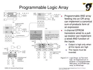
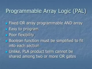
Programmable Array Logic (PAL). Fixed OR array programmable AND array Easy to program Poor flexibility Boolean function must be simplified to fit into each section Unlike, PLA product term cannot be shared among two or more OR gates. PAL with 4-input 4-output 3-wide AND-OR structure.

Programmable Array Logic (PAL)
E N D
Presentation Transcript
Programmable Array Logic (PAL) • Fixed OR array programmable AND array • Easy to program • Poor flexibility • Boolean function must be simplified to fit into each section • Unlike, PLA product term cannot be shared among two or more OR gates
Use PAL to design combinational logic circuit • Boolean function • simplified • PAL programming table is similar to that of PLA except that only inputs of AND gates need to be programmed.
Sequential Programmable Device • Digital systems are designed using flip-flop and gates • PLD contains only gates • Sequential Programmable Device include both flip-flop and gates • Three major types: 1. Sequential (simple) programmable logic device (SPLD) 2. Sequential programmable logic device (CPLD) 3. Field programmable gate array (FPGA)
SPLD • SPLD: AND-OR array + F.F. (See Fig. 7-18) • Output can be taken from OR gates or output of F.F. • F.F. can be D or JK • Each section is called macrocell include sum-of-product combinational logic and a F.F. • Typically include 8-10 macrocell in a chip (IC)
Field-programmable logic sequential (FPLS) • First programmable device developed to support sequential circuits • PLA + several F.F. (programmable to D or JK) • Did not succeed commercially because it has to many programmable connection
Complex PLD (CPLD) • Collection of several individual PLD • Fig. 7-20 shows a general configuration of CPLD • PLD is interconnected through programmable switch matrix • I/O blocks provide the connection to IC pin • Each I/O is driven by 3-state buffer and can be programmed to act as input or output • The programmable switch matrix receives input from I/O block and directs it to the individual macrocell
Field Programmable Gate Array (FPGA) • VLSI • Elementary element is logic block • Consists hundreds or thousands logic block • Logic block consists of look-up table, multiplexers, gates and F.F. • Look-up table is a truth table stored in a SRAM and provides the combinational function for the logic block • Remember that PAL or PLA is used for macrocell in CPLD
FPGA • Use RAM instead of ROM • Advantage: programmable • Disadvantage: volatile • PLD, CPLD, FPGA requires CAD • Schematic • HDL • VHDL • Verilog HDL
Exercise • 7-1, 7-2, 7-4, 7-6, 7-8, 7-9, 7-15, 7-17, 7-18, 7-19, 7-20, 7-21, 7-24, 7-25