Programmable Configurations
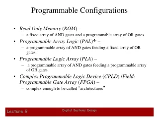
Programmable Configurations. Read Only Memory ( ROM ) – a fixed array of AND gates and a programmable array of OR gates Programmable Array Logic ( PAL ) Ò – a programmable array of AND gates feeding a fixed array of OR gates. Programmable Logic Array ( PLA ) –

Programmable Configurations
E N D
Presentation Transcript
Programmable Configurations • Read Only Memory (ROM) – • a fixed array of AND gates and a programmable array of OR gates • Programmable Array Logic (PAL)Ò – • a programmable array of AND gates feeding a fixed array of OR gates. • Programmable Logic Array (PLA) – • a programmable array of AND gates feeding a programmable array of OR gates. • Complex Programmable Logic Device (CPLD) /Field- Programmable Gate Array (FPGA) – • complex enough to be called “architectures” KU College of Engineering Elec 204: Digital Systems Design
ROM, PAL and PLA Configurations Fixed Programmable Programmable Inputs Outputs AND array Connections OR array (decoder) (a) Programmable read-only memory (PROM) Programmable Programmable Fixed Inputs Outputs Connections AND array OR array (b) Programmable array logic (PAL) device Programmable Programmable Programmable Programmable Outputs Inputs Connections Connections AND array OR array (c) Programmable logic array (PLA) device KU College of Engineering Elec 204: Digital Systems Design
Read Only Memory • Read Only Memories (ROM) or Programmable Read Only Memories (PROM) have: • N input lines, • M output lines, and • 2N decoded minterms. • Fixed AND array with 2N outputs implementing all N-literal minterms. • Programmable OR Array with M outputs lines to form up to M sum of minterm expressions. • A program for a ROM or PROM is simply a multiple-output truth table • If a 1 entry, a connection is made to the corresponding minterm for the corresponding output • If a 0, no connection is made KU College of Engineering Elec 204: Digital Systems Design
X X X D7 D6 X X D5 X D4 D3 A2 A X D2 X X B A1 D1 X A0 D0 C F0 F2 F1 F3 Read Only Memory Example • Example: A 8 X 4 ROM (N = 3 input lines, M= 4 output lines) • The fixed "AND" array is a“decoder” with 3 inputs and 8outputs implementing minterms. • The programmable "OR“array uses a single line torepresent all inputs to anOR gate. An “X” in thearray corresponds to attaching theminterm to the OR • Read Example: For input (A2,A1,A0)= 011, output is (F3,F2,F1,F0 ) = 0011. • What are functions F3, F2 , F1 and F0 in terms of (A2, A1, A0)? KU College of Engineering Elec 204: Digital Systems Design
Programmable Array Logic (PAL) • The PAL is the opposite of the ROM, having a programmable set of ANDs combined with fixed ORs. • Disadvantage • ROM guaranteed to implement any M functions of Ninputs. PAL may have too few inputs to the OR gates. • Advantages • For given internal complexity, a PAL can have larger N and M • Some PALs have outputs that can be complemented, adding POS functions • No multilevel circuit implementations in ROM (without external connections from output to input). PAL hasoutputs from OR terms as internal inputs to all ANDterms, making implementation of multi-level circuits easier. KU College of Engineering Elec 204: Digital Systems Design
AND gates inputs 0 1 2 3 4 5 6 7 8 9 Product 1 X term F 2 1 X X 3 I A = 1 4 X X X F 5 2 X X 6 X X I B = 2 7 X X F 8 3 X X 9 X I C = 3 10 X X F 11 4 X X 12 X I 4 = D 0 1 2 3 4 5 6 7 8 9 Programmable Array Logic Example • 4-input, 3-output PAL with fixed, 3-input OR terms • What are the equations for F1 through F4? F1 = C’ + A’B’ F2 = A’BC’ + AC + AB’ F3 = AD + BD + F1 F4 = AB + CD + F1’ KU College of Engineering Elec 204: Digital Systems Design
Programmable Logic Array (PLA) • Compared to a ROM and a PAL, a PLA is the most flexible having a programmable set of ANDs combined with a programmable set of ORs. • Advantages • A PLA can have large N and M permitting implementation of equations that are impractical for a ROM (because of the number of inputs, N, required • A PLA has all of its product terms connectable to all outputs, overcoming the problem of the limited inputs to the PAL ORs • Some PLAs have outputs that can be complemented, adding POS functions • Disadvantage • Often, the product term count limits the application of a PLA. Two-level multiple-output optimization reduces the number of product terms in an implementation, helping to fit it into a PLA. KU College of Engineering Elec 204: Digital Systems Design
A B C A B X 1 X X X B C X X 2 X Fuse intact X Fuse blown A C X 3 X X A B X X 4 X X 0 C C B B A A 1 X F 1 F 2 Programmable Logic Array Example • What are the equations for F1 and F2? • Could the PLA implement the functions without the XOR gates? • 3-input, 3-output PLA with 4 product terms KU College of Engineering Elec 204: Digital Systems Design
Combinational Functions and Circuits • Rudimentary logic functions • Decoding • Encoding • Selecting KU College of Engineering Elec 204: Digital Systems Design
V or V CC DD 1 F = 1 F = 1 X F = X (c) 0 F = 0 F = 0 X F = X (a) (b) (d) Rudimentary Logic Functions • Functions of a single variable X • Can be used on theinputs to functionalblocks to implementother than the block’sintended function KU College of Engineering Elec 204: Digital Systems Design
A A Multiple-bit Rudimentary Functions F 3 2 3 1 2:1 F(2:1) 2 F 1 4 4 2 • Multi-bit Examples: • A wide line is used to represent a bus which is a vector signal • In (b) of the example, F = (F3, F2, F1, F0) is a bus. • The bus can be split into individual bits as shown in (b) • Sets of bits can be split from the bus as shown in (c) for bits 2 and 1 of F. • The sets of bits need not be continuous as shown in (d) for bits 3, 1, and 0 of F. F F 0 0 F 1 1 0 (c) A A F 0 3 (a) (b) 3,1:0 F(3), F(1:0) 4 F (d) KU College of Engineering Elec 204: Digital Systems Design
Enabling Function • Enabling permits an input signal to pass through to an output • Disabling blocks an input signal from passing through to an output, replacing it with a fixed value • The value on the output when it is disable can be Hi-Z (as for three-state buffers and transmission gates), 0 , or 1 • When disabled, 0 output • When disabled, 1 output KU College of Engineering Elec 204: Digital Systems Design
Decoders • Multiple-input multiple-output logic circuit which maps coded inputs to coded outputs • n input bits can code upto 2n different output bits • n-to-m decoder: maps n-bit input to m-bit output where m < 2n KU College of Engineering Elec 204: Digital Systems Design
Decoders • General decoder structure • Typically n inputs, 2n outputs • 2-to-4, 3-to-8, 4-to-16, etc. KU College of Engineering Elec 204: Digital Systems Design
Note “x” (don’t care) notation. Binary 2-to-4 decoder KU College of Engineering Elec 204: Digital Systems Design
2-to-4-decoder logic diagram m0=I1’I0’ m1=I1’I0 m2=I1I0’ m3=I1I0 KU College of Engineering Elec 204: Digital Systems Design
Decoder Expansion 3-to-8 decoder out of 2 2-to-4 decoders with enable KU College of Engineering Elec 204: Digital Systems Design
Decoder and OR Gate Implementation of a Binary Adder • Arithmetic sum of three bits X,Y,Z • Output pair (C,S) S(X,Y,Z) = C(X,Y,Z) = KU College of Engineering Elec 204: Digital Systems Design
S(X,Y,Z) = C(X,Y,Z) = KU College of Engineering Elec 204: Digital Systems Design
Decoder Applications • Microprocessor memory systems • Selecting different banks of memory • Microprocessor input/output systems • Selecting different devices • Microprocessor instruction decoding • Enabling different functional units • Memory chips • Enabling different rows of memory depending on address • Lots of other applications • Seven segment decoder, 4-to-7 decoder KU College of Engineering Elec 204: Digital Systems Design
Decoder Encoder Encoders vs. Decoders KU College of Engineering Elec 204: Digital Systems Design
Binary encoders KU College of Engineering Elec 204: Digital Systems Design
Need priority in most applications KU College of Engineering Elec 204: Digital Systems Design
Priority Encoder KU College of Engineering Elec 204: Digital Systems Design
A0 = D3 + D1D2’ A1 = D2 + D3 V = D0 + D1 + D2 + D3 KU College of Engineering Elec 204: Digital Systems Design
Another approach to the design of 8-input priority encoder KU College of Engineering Elec 204: Digital Systems Design
Priority-encoder logic equations KU College of Engineering Elec 204: Digital Systems Design
Selecting • Selecting of data or information is a critical function in digital systems and computers • Circuits that perform selecting have: • A set of information inputs from which the selection is made • A single output • A set of control lines for making the selection • Logic circuits that perform selecting are called multiplexers • Selecting can also be done by three-state logic or transmission gates KU College of Engineering Elec 204: Digital Systems Design
Multiplexers • MUX: • Selects binary information from one of many input lines and directs the information to a single output line. • Selection of a particular input is controlled by a set of input variables. • # of selection control bits: n • # of possible input lines: 2n • # of output: 1 2n-to-1 MUX KU College of Engineering Elec 204: Digital Systems Design
Multiplexers KU College of Engineering Elec 204: Digital Systems Design
4-to-1-Line MUX KU College of Engineering Elec 204: Digital Systems Design
Quadruple 2-to-1-Line MUX KU College of Engineering Elec 204: Digital Systems Design
Combinational Circuit ImplementationUsing MUX F(X,Y,Z)=m(1,2,6,7) using a 4-to-1 MUX KU College of Engineering Elec 204: Digital Systems Design
F(A,B,C,D)=m(1,3,4,11,12,13,14,15) KU College of Engineering Elec 204: Digital Systems Design
Demultiplexer • Inverse of the MUX • Receives information from a single line and transmits it to one of the 2n possible output lines • 1-to-4-Line DMUX / 2-to-4-Line Decoder KU College of Engineering Elec 204: Digital Systems Design
Binary Adders • Arithmetic circuits: • combinational circuits with add, subt, mult & div. • Present a hierarchical design • Simple addition of two bits • 0+0 = 02, 0+1 = 12, 1+0 = 12 and 1+1 = 102 • Half Adder: • Combinational circuit that adds two bits • Full Adder: • Combinational circuit that adds three bits (two input, one carry) KU College of Engineering Elec 204: Digital Systems Design
Half Adder • Sum of two binary digits S=X’Y+XY’ C=XY KU College of Engineering Elec 204: Digital Systems Design
Full Adder • Sum of three binary digits KU College of Engineering Elec 204: Digital Systems Design
Logic Diagram for Full Adder XY Z Z(XY) XY XY + Z(XY) KU College of Engineering Elec 204: Digital Systems Design
Binary Ripple Carry Adder • The parallel adder of n binary full adders • Carry out Carry in of next full adder KU College of Engineering Elec 204: Digital Systems Design
Carry Lookahead Adder • Ripple carry adder • Simple but has a long circuit delay • Define a partial full adder • Try to lower gate delays for ripple carry adder KU College of Engineering Elec 204: Digital Systems Design
Binary Adder/Subtractor KU College of Engineering Elec 204: Digital Systems Design
Overflow • When does it occur? • How do we detect it? 01110 10000 + 5 0101 -4 1100 + 7 0111 -6 1010 +12 ? 01100 -10 ? 10110 KU College of Engineering Elec 204: Digital Systems Design
Binary Multipliers KU College of Engineering Elec 204: Digital Systems Design
4-bit by 3-bit multiplier KU College of Engineering Elec 204: Digital Systems Design