Download
1 / 45
530 likes | 1.08k Views
Raman Spectroscopy of Nanostructures. EE 235 16 March 2009. Raman studies of nanostructures. Multiple meanings! Study of the nanostructures themselves Study of a chemical analyte on top of nanostructures. Outline. General principles Light scattering

E N D
Raman Spectroscopy of Nanostructures EE 235 16 March 2009
Raman studies of nanostructures Multiple meanings! • Study of the nanostructures themselves • Study of a chemical analyte on top of nanostructures
Outline • General principles • Light scattering • Electronic and vibrational energy levels • Experimental implementation • Raman scattering in crystals • Resonant enhancement • Signal enhancement • Resonant enhancement • Surface enhancement (SERS)
Outline • General principles • Light scattering • Electronic and vibrational energy levels • Experimental implementation • Raman scattering in crystals • Resonant enhancement • Signal enhancement • Resonant enhancement • Surface enhancement (SERS)
Optical options l l0 • Raman scattering: Inelastic light scattering Incident light l0 Absorbed Transmitted l0 l0 Reflected Elastic l0 Scattered l l0 Inelastic
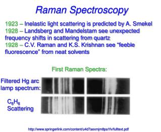
Light scattering Rayleigh: Elastic scattering Raman: Inelastic scattering www.phy.cam.ac.uk/history/historypictures/LordRayleigh.jpg www.iisc.ernet.in/images/CVRaman.gif
Elastic scattering Electronic excited state E=E0cos(wit) + Induced polarization P = E (: polarizability) - + “Virtual state” - r0 r Dipole re-radiates at same frequency wi Electronic ground state
- + - + - + Inelastic scattering Vibration changes polarizability: r0 a0 m1 m2 Periodic displacement a|Qmax wvib a|Qmin Frequency of scattered light differs from the incident light by an amount corresponding to a normal mode of the mechanical oscillator
Classical scattering model Induced polarizability change from vibrations (first order) Taylor expand Rayleigh term: Raman term: Stokes Anti-Stokes
O C O Energy scales • Visible light (red), 620 nm ↔ 2 eV ↔ 484 THz ↔ 16130 cm-1 • CO2 symmetric mode, 1335 cm-1↔ 41 THz ↔ 0.165 eV ↔ 7.5 mm Vibrational energies << Optical energies
Scattering processes Energy Electronic excited state Raman Rayleigh Vibrational levels Electronic ground state FIR- MIR Stokes Anti-Stokes
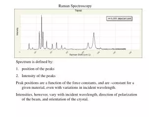
Scattering spectroscopy • Measure the wavelength-shifted scattered light as a probe of vibrational energies • Known characteristic bond frequencies
Scattering spectroscopy • Measure the wavelength-shifted scattered light as a probe of vibrational energies • Known characteristic bond frequencies • “Chemical fingerprinting”: every molecule has a unique vibrational spectrum
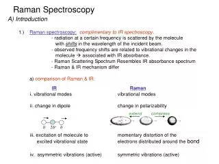
Chemical fingerprinting • IR absorption and Raman scattering complementary • Same transitions, different selection rules - all has to do with symmetry cm-1
Scattering spectroscopy • “Chemical fingerprinting”: every molecule has a unique vibrational spectrum • Check the aptly-named Journal of Raman spectroscopy: • Chemical analysis tool! http://www3.interscience.wiley.com/journal/3420/home
Outline • General principles • Light scattering • Electronic and vibrational energy levels • Experimental implementation • Raman in crystals • Resonant enhancement • Signal enhancement • Resonant enhancement • Surface enhancement (SERS)
In principle, any laser wavelength shorter (i.e. higher energy) than the vibrational mode of interest will work as a source Scattering processes Energy Electronic excited state Raman Rayleigh Vibrational levels Electronic ground state FIR- MIR Stokes Anti-Stokes
O C O Implementation issues • Weak Raman-scattered light close to strong source laser + Rayleigh-scattered light • Need high rejection of unwanted “carrier frequency” light very close to Raman-shifted signal light 2 eV Intensity 0.165 eV eV
Spectrometer Implementation issues • Need: very clean source line • Very sharp edge discrimination Dispersive stage Sample Filter Detector Narrow excitation source
Spectrometer3 Spectrometer1 Spectrometer2 Raman instrumentation • Multi-stage spectrographs Disperse Recompress Disperse Input Detector • Excellent stray light rejection, can measure very close to laser line (few cm-1) • Large and expensive
Spectrometer Detector Raman instrumentation • Single spectrometer, strong filters • Longpass filter in collection path • Line-pass filter (shortpass for tunable lasers) for laser line clean-up in excitation path • Final resolution depends on spectrograph and detector; filter limitation ~tens of cm-1 Input Long-pass filter to transmit only Stokes-scattered light semrock LP-633RE
micro-Raman spectroscopy • Spatial imaging down to diffraction limit of excitation wavelength used • Confocal setup - small sample volume probed • Vibrational map of sample JobinYvon
Outline • General principles • Light scattering • Electronic and vibrational energy levels • Experimental implementation • Raman scattering in crystals • Resonant enhancement • Signal enhancement • Resonant enhancement • Surface enhancement (SERS)
[111] c-axis: [0001] Raman scattering in crystals • Vibrational modes in crystals: phonons • Symmetry considerations = entire field of physics! Wurtzite: hexagonal crystal e.g. II-VI and III-Nitrides semiconductors: ZnO, ZnS, CdSe, GaN, etc. Zincblende: cubic crystal e.g. III-V semiconductors: usual for III-Arsenides and III-Antimonides, sometimes also III-Nitrides
[0001] c-axis || c ┴c ┴c ┴c Raman scattering in crystals • Wurtzite crystal: hexagonal structure • Anisotropic crystal: Material properties like refractive index, effective masses depend on direction relative to c-axis N Ga N “optical axis” Ga • Restoring forces for crystal vibrations also have c-axis dependence
Wurtzite crystal modes c-axis Displacement of atoms || c-axis: A and B modes Displacement of atoms ┴c-axis: E-modes N Ga E1 A1 E2(2) E2(1) B1(1) B1(2) Polar (TO - LO splitting) Polar (TO - LO splitting) Non-polar Non-polar
Wurtzite crystal modes c-axis N Ga E1 A1 E2(2) E2(1) B1(1) B1(2) • Vibrational mode measured depends on form of tensor for a given measurement geometry
N Ga Raman mode polarization • Vibrational mode measured depends on form of tensor for a given measurement geometry c-axis || z “A1“ Ei || z ki ks Es || z
N Ga Raman mode polarization • Vibrational mode measured depends on form of tensor for a given measurement geometry • Cross-polarized measurement gives no mode at this “A1” frequency c-axis || z “A1“ Ei || z ki ks Es || z Es ┴z
N Ga Raman mode polarization • Different mode, different intensity growth axis is not c-axis “A1“ Ei || z ki ks Es ┴z
Summary: Raman in crystals • Measurement geometry / polarizations determine which modes can be Raman-scattered • This example was looking at how one particular mode (A1) would change • 1) Knowing the nanowire direction but under different measurement geometries • 2) Not knowing crystal orientation: use mode selection to determine • Non-destructive structural characterization tool for nanostructures! For example:
Outline • General principles • Light scattering • Electronic and vibrational energy levels • Experimental implementation • Raman scattering in crystals • Resonant enhancement • Signal enhancement • Resonant Raman - good or bad? • Surface-enhancement (SERS)
Electronic resonance Energy Electronic excited state Resonant Raman: effective cross-section increased ~10-105 from non-resonant case (comparable to Rayleigh scattering!) UV / VIS / NIR Vibrational levels Electronic ground state FIR- MIR Stokes
Resonant Raman - GaAs nanocrystals • NIR used as excitation source, close to PL spectrum T = 1.2 K Excitation laser LO phonon Photoluminescence Raman-scattered phonon: follows laser energy 2-phonon process PL: no change in energy if laser wavelength changes
Resonant Raman - GaAs nanocrystals • Track intensity of single vibrational mode over laser excitation tuning range of electronic resonance Outgoing resonance: Scattered phonon energy matches electronic transition Intensity of 294 cm-1 GaAs line Incoming resonance: Laser energy = electronic transition
Resonant Raman • Why not do this all the time? • Energy of electronic resonance distinct from scattering process, does not follow laser (e.g. semiconductor bandgap) • Excitation source must match electronic resonance • Much easier to match with tunable lasers (not readily available in the UV/VIS) • Could enhance a few particular lines, overwhelm others?
Resonant Raman • Entirely sample-dependent. Chemical analysis: fluorescence always a bad word! end up choosing laser wavelength to avoid fluorescence
Outline • General principles • Light scattering • Electronic and vibrational energy levels • Experimental implementation • Raman scattering in crystals • Resonant enhancement • Signal enhancement • Resonant enhancement • Surface enhancement (SERS)
1974: Pyridine on rough silver surface • Wet experiment; silver electrode ended up etched • No great claims of enhancement; were interested in type of bond to Ag surface
1974: Pyridine on Ag surfaces • Authors focus on middle peak to propose bond model • Intensity increases more than can be accounted for with surface roughening Increasing voltage on Ag electrode
1977: Pyridine on Ag surfaces • Proposed EM mechanism related to “hot spots” on metal surface
Skip forward 30 years… • How to engineer “hot spots”? • Very active area of research • Increased Raman signal by >107 via EM field enhancements • Much lower excitation laser power requirements • Roughened metal surfaces, sharp-tipped metallic structures, bow-tie substrates • Also: “Tip-enhanced Raman scattering” (TERS) using NSOM • Jeff Neaton (LBL) - next week, Raman/SERS theory • Luke Lee (BioE) - 2 weeks, SERS experimental work
r0 Mid- to far-infrared Energy scales E n = 2 Electronic level n = 1 r Vibrational levels Rotational levels (microwave) r0
Energy scales Acoustic Radio Micro FIR NIR VIS UV X-ray g-ray Nuclear spins (NMR) Electron spins (ESR), rotational levels Core electron levels Vibrational levels Electronic levels