Chapter 2 Solid-State Electronics
Chapter 2 Solid-State Electronics. Microelectronic Circuit Design Richard C. Jaeger Travis N. Blalock. Chapter Goals. Explore semiconductors and discover how engineers control semiconductor properties to build electronic devices.

Chapter 2 Solid-State Electronics
E N D
Presentation Transcript
Chapter 2Solid-State Electronics Microelectronic Circuit Design Richard C. JaegerTravis N. Blalock Microelectronic Circuit Design McGraw-Hill
Chapter Goals • Explore semiconductors and discover how engineers control semiconductor properties to build electronic devices. • Characterize resistivity of insulators, semiconductors, and conductors. • Develop covalent bond and energy band models for semiconductors. • Understand band gap energy and intrinsic carrier concentration. • Explore the behavior of electrons and holes in semiconductors. • Discuss acceptor and donor impurities in semiconductors. • Learn to control the electron and hole populations using impurity doping. • Understand drift and diffusion currents in semiconductors. • Explore low-field mobility and velocity saturation. • Discuss the dependence of mobility on doping level. Microelectronic Circuit Design McGraw-Hill
The Inventors of the Integrated Circuit Andy Grove, Robert Noyce, and Gordon Moore with Intel 8080 layout. Jack Kilby Microelectronic Circuit Design McGraw-Hill
The Kilby Integrated Circuit Semiconductor die Active device Electrical contacts Microelectronic Circuit Design McGraw-Hill
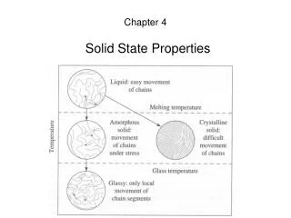
Solid-State Electronic Materials • Electronic materials fall into three categories: • Insulators Resistivity () > 105-cm • Semiconductors 10-3 < < 105 -cm • Conductors < 10-3 -cm • Elemental semiconductors are formed from a single type of atom • Compound semiconductors are formed from combinations of column III and V elements or columns II and VI. • Germanium was used in many early devices. • Silicon quickly replaced germanium due to its higher bandgap energy, lower cost, and is easily oxidized to form silicon-dioxide insulating layers. Microelectronic Circuit Design McGraw-Hill
Semiconductor Materials (cont.) Microelectronic Circuit Design McGraw-Hill
Covalent Bond Model Silicon diamond lattice unit cell. 3D Animation Corner of diamond lattice showing four nearest neighbor bonding. View of crystal lattice along a crystallographic axis. Microelectronic Circuit Design McGraw-Hill
Silicon Covalent Bond Model (cont.) Near absolute zero, all bonds are complete. Each Si atom contributes one electron to each of the four bond pairs. Increasing temperature adds energy to the system and breaks bonds in the lattice, generating electron-hole pairs. Microelectronic Circuit Design McGraw-Hill
Intrinsic Carrier Concentration • The density of carriers in a semiconductor as a function of temperature and material properties is: • EG = semiconductor bandgap energy in eV (electron volts) • k = Boltzmann’s constant, 8.62 x 10⁻⁵ eV/K • T = absolute temperature, K • B = material-dependent parameter, 1.08 x 1031 K-3 cm-6 for Si • Bandgap energy is the minimum energy needed to free an electron by breaking a covalent bond in the semiconductor crystal. Microelectronic Circuit Design McGraw-Hill
Intrinsic Carrier Concentration (cont.) • Electron density is n (electrons/cm3) and ni for intrinsic material n = ni. • Intrinsic refers to properties of pure materials. • ni ≈ 1010 cm-3 for Si Microelectronic Circuit Design McGraw-Hill
Electron-hole concentrations • A vacancy is left when a covalent bond is broken. • The vacancy is called a hole. • A hole moves when the vacancy is filled by an electron from a nearby broken bond (hole current). • Hole density is represented by p. • For intrinsic silicon, n = ni = p. • The product of electron and hole concentrations is pn = ni2. • The pn product above holds when a semiconductor is in thermal equilibrium (not with an external voltage applied). Microelectronic Circuit Design McGraw-Hill
Drift Current • Electrical resistivity and its reciprocal, conductivity , characterize current flow in a material when an electric field is applied. • Charged particles move or drift under the influence of the applied field. • The resulting current is called drift current. • Drift current density is j=Qv (C/cm3)(cm/s) = A/cm2 j = current density, (Coulomb charge moving through a unit area) Q = charge density, (Charge in a unit volume) v = velocity of charge in an electric field. Note that “density” may mean area or volumetric density, depending on the context. Generation, Drift , Diffusion and Recombination Animation Microelectronic Circuit Design McGraw-Hill
Mobility • At low fields, carrier drift velocity v (cm/s) is proportional to electric field E (V/cm). The constant of proportionality is the mobility, : • vn = - nE and vp = pE , where • vn and vp = electron and hole velocity (cm/s), • n and p = electron and hole mobility (cm2/Vs) • Hole mobility is less than electron since hole current is the result of multiple covalent bond disruptions, while electrons can move freely about the crystal. Microelectronic Circuit Design McGraw-Hill
Velocity Saturation At high fields, carrier velocity saturates and places upper limits on the speed of solid-state devices. Microelectronic Circuit Design McGraw-Hill
Intrinsic Silicon Resistivity • Given drift current and mobility, we can calculate resistivity: jndrift = Qnvn = (-qn)(- nE) = qn nE A/cm2 jpdrift = Qpvp = (qp)( pE) = qp pE A/cm2 jTdrift =jn + jp = q(n n + p p)E = E This defines electrical conductivity: = q(n n + p p) (cm)-1 Resistivity is the reciprocal of conductivity: = 1/ (cm) Microelectronic Circuit Design McGraw-Hill
Problem: Find the resistivity of intrinsic silicon at room temperature and classify it as an insulator, semiconductor, or conductor. Solution: Known Information and Given Data: The room temperature mobilities for intrinsic silicon were given right after Eq. 2.5. For intrinsic silicon, the electron and hole densities are both equal to ni. Unknowns: Resistivity and classification. Approach: Use Eqs. 2.8 and 2.9. [ = q(n n + p p) (cm)-1] Assumptions: Temperature is unspecified; assume “room temperature” with ni = 1010/cm3. Analysis: Next slide… Example: Calculate the resistivity of intrinsic silicon Microelectronic Circuit Design McGraw-Hill
Analysis: Charge density of electrons is Qn = -qni and for holes is Qp = +qni. Substituting into Eq. 2.8: = (1.60 x 10⁻¹⁹)[(1010)(1350) + (1010)(500)] (C)(cm-3)(cm2/Vs) = 2.96 x 10⁻⁶(cm)-1 ---> = 1/ = 3.38 x 105cm From Table 2.1, intrinsic silicon is near the low end of the insulator resistivity range Check of Results: Resistivity has been found, and intrinsic silicon is a poor insulator. Example: Calculate the resistivity of intrinsic silicon (cont.) Microelectronic Circuit Design McGraw-Hill
Strained Silicon • Strained Silicon increases transistor drive current which improves switching speed by making current flow more smoothly. • Has negligible effect on manufacturing cost. • Used in 90 nm process for Prescott and Dothan Microelectronic Circuit Design McGraw-Hill
Strained Silicon Microelectronic Circuit Design McGraw-Hill
Semiconductor Doping • Doping is the process of adding very small well controlled amounts of impurities into a semiconductor. • Doping enables the control of the resistivity and other properties over a wide range of values. • For silicon, impurities are from columns III and V of the periodic table. Microelectronic Circuit Design McGraw-Hill
Donor Impurities in Silicon • Phosphorous (or other column V element) atom replaces silicon atom in crystal lattice. • Since phosphorous has five outer shell electrons, there is now an ‘extra’ electron in the structure. • Material is still charge neutral, but very little energy is required to free the electron for conduction since it is not participating in a bond. Microelectronic Circuit Design McGraw-Hill
Acceptor Impurities in Silicon • Boron (column III element) has been added to silicon. • There is now an incomplete bond pair, creating a vacancy for an electron. • Little energy is required to move a nearby electron into the vacancy. • As the ‘hole’ propagates, charge is moved across the silicon. Microelectronic Circuit Design McGraw-Hill
Acceptor Impurities in Silicon (cont.) Hole is propagating through the silicon. Microelectronic Circuit Design McGraw-Hill
Doped Silicon Carrier Concentrations • If n > p, the material is n-type.If p > n, the material is p-type. • The carrier with the largest concentration is the majority carrier, the smaller is the minority carrier. • ND = donor impurity concentration atoms/cm3NA = acceptor impurity concentration atoms/cm3 • Charge neutrality requires q(ND + p - NA - n) = 0 • It can also be shown that pn = ni2, even for doped semiconductors in thermal equilibrium. Microelectronic Circuit Design McGraw-Hill
n-type Material • Substituting p=ni2/n into q(ND + p - NA - n) = 0 yields n2 - (ND - NA)n - ni2 = 0. • Solving for n • For (ND - NA) >> 2ni, n (ND - NA) . Microelectronic Circuit Design McGraw-Hill
p-type Material • Similar to the approach used with n-type material we find the following equations: • We find the majority carrier concentration from charge neutrality (Eq. 2.10) and find the minority carrier conc. from the thermal equilibrium relationship (Eq. 2.3). • For (NA - ND) >> 2ni, p (NA - ND) . Microelectronic Circuit Design McGraw-Hill
Practical Doping Levels • Majority carrier concentrations are established at manufacturing time and are independent of temperature (over practical temp. ranges). • However, minority carrier concentrations are proportional to ni2, a highly temperature dependent term. • For practical doping levels, n (ND - NA) for n-type and p (NA - ND) for p-type material. • Typical doping ranges are 1014/cm3 to 1021/cm3. Microelectronic Circuit Design McGraw-Hill
Mobility and Resistivity in Doped Semiconductors Microelectronic Circuit Design McGraw-Hill
Diffusion Current • In practical semiconductors, it is quite useful to create carrier concentration gradients by varying the dopant concentration and/or the dopant type across a region of semiconductor. • This gives rise to a diffusion current resulting from the natural tendency of carriers to move from high concentration regions to low concentration regions. • Diffusion current is analogous to a gas moving across a room to evenly distribute itself across the volume. Microelectronic Circuit Design McGraw-Hill
Diffusion Current (cont.) • Carriers move toward regions of lower concentration, so diffusion current densities are proportional to the negative of the carrier gradient. Diffusion currents in the presence of a concentration gradient. Diffusion current density equations Microelectronic Circuit Design McGraw-Hill
Diffusion Current (cont.) • Dp and Dn are the hole and electron diffusivities with units cm2/s. Diffusivity and mobility are related by Einsteins’s relationship: • The thermal voltage, VT =kT/q, is approximately 25 mV at room temperature. We will encounter VT throughout this book. Microelectronic Circuit Design McGraw-Hill
Total Current in a Semiconductor • Total current is the sum of drift and diffusion current:Rewriting using Einstein’s relationship (Dp=nVT), In the following chapters, we will use these equations, combined with Gauss’ law, (E)=Q, to calculate currents in a variety of semiconductor devices. Microelectronic Circuit Design McGraw-Hill
Semiconductor Energy Band Model Thermal energy breaks covalent bonds and moves the electrons up into the conduction band. Semiconductor energy band model. EC and EV are energy levels at the edge of the conduction and valence bands. Electron participating in a covalent bond is in a lower energy state in the valence band. This diagram represents 0 K. Microelectronic Circuit Design McGraw-Hill
Energy Band Model for a Doped Semiconductor Semiconductor with donor or n-type dopants. The donor atoms have free electrons with energy ED. Since ED is close to EC, (about 0.045 eV for phosphorous), it is easy for electrons in an n-type material to move up into the conduction band. Semiconductor with acceptor or p-type dopants. The acceptor atoms have unfilled covalent bonds with energy state EA. Since EA is close to EV, (about 0.044 eV for boron), it is easy for electrons in the valence band to move up into the acceptor sites and complete covalent bond pairs. Microelectronic Circuit Design McGraw-Hill
Energy Band Model for Compensated Semiconductor The combination of the covalent bond model and the energy band models are complementary and help us visualize the hole and electron conduction processes. A compensated semiconductor has both n-type and p-type dopants. If ND > NA, there are more ND donor levels. The donor electrons fill the acceptor sites. The remaining ND-NA electrons are available for promotion to the conduction band. Microelectronic Circuit Design McGraw-Hill
Energy Band Model • Energy Band Model Animation Microelectronic Circuit Design McGraw-Hill
Youtube animations • *Investing in Chip Making Innovation -- Inside Intel's Fab - here • Silicon Wafer Processing – here • How do they make wafers and computer chips – here • From Fab to Test : AMD’s 45nm process – here • 45nm – what does it mean – here • Get inside a Intel 45nm fab - here Microelectronic Circuit Design McGraw-Hill
Growing Silicon Ingot Microelectronic Circuit Design McGraw-Hill
Integrated Circuit Fabrication Overview Top view of an integrated pn diode. Microelectronic Circuit Design McGraw-Hill
Integrated Circuit Fabrication (cont.) (a) First mask exposure, (b) post-exposure and development of photoresist, (c) after SiO2 etch, and (d) after implantion/diffusion of acceptor dopant. Microelectronic Circuit Design McGraw-Hill
Integrated Circuit Fabrication (cont.) (e) Exposure of contact opening mask, (f) after resist development and etching of contact openings, (g) exposure of metal mask, and (h) After etching of aluminum and resist removal. Microelectronic Circuit Design McGraw-Hill
Micrograph of diode • Diode Fabrication Animation Microelectronic Circuit Design McGraw-Hill
Lab-on-a-chip Microelectronic Circuit Design McGraw-Hill
Lab-on-a-chip (cont.) Microelectronic Circuit Design McGraw-Hill
Homework 2 • 2.4 • 2.5 • 2.16 • 2.32 • 2.49 • 2.51 Microelectronic Circuit Design McGraw-Hill
End of Chapter 2 Microelectronic Circuit Design McGraw-Hill