Download
1 / 1
10 likes | 105 Views
Abstract.

E N D
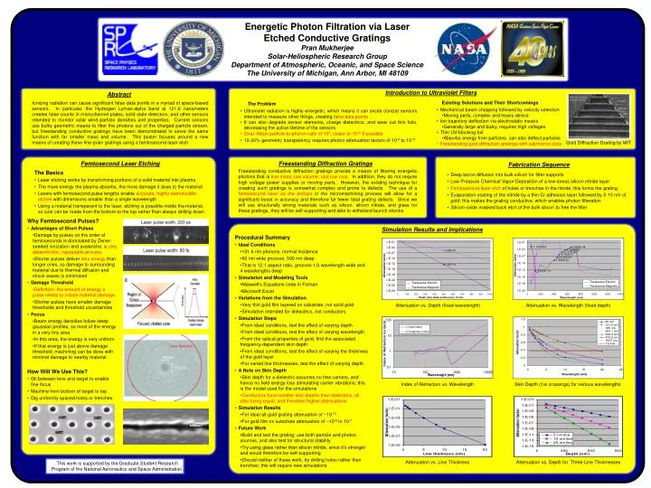
Abstract Ionizing radiation can cause significant false data points in a myriad of space-based sensors. In particular, the Hydrogen Lyman-alpha band at 121.6 nanometers creates false counts in microchannel plates, solid state detectors, and other sensors intended to monitor solar wind particle densities and properties. Current sensors use bulky geometric means to filter the photons out of the charged particle stream, but freestanding conductive gratings have been demonstrated to serve the same function with far smaller mass and volume. This poster focuses around a new means of creating these fine-grain gratings using a femtosecond laser etch. The Problem Existing Solutions and Their Shortcomings • Ultraviolet radiation is highly energetic, which means it can excite (ionize) sensors intended to measure other things, creating false data points • It can also degrade sensor elements, charge dielectrics, and wear out thin foils, decreasing the active lifetime of the sensors • Goal: Attain particle-to-photon ratio of 105, closer to 1010 if possible • 10-30% geometric transparency requires photon attenuation factors of 10-6 to 10-11 • Mechanical beam chopping followed by velocity selection • Moving parts, complex and heavy device • Ion trajectory deflection via electrostatic means • Generally large and bulky, requires high voltages • Thin UV-blocking foil • Absorbs energy from particles, can also deflect particles • Freestanding gold diffraction gratings with submicron slots Gold Diffraction Grating by MIT This work is supported by the Graduate Student Research Program of the National Aeronautics and Space Administration. Energetic Photon Filtration via Laser Etched Conductive Gratings Pran Mukherjee Solar-Heliospheric Research Group Department of Atmospheric, Oceanic, and Space Science The University of Michigan, Ann Arbor, MI 48109 Introduction to Ultraviolet Filters Femtosecond Laser Etching Freestanding Diffraction Gratings Fabrication Sequence Freestanding conductive diffraction gratings provide a means of filtering energetic photons that is low mass, low volume, and low cost. In addition, they do not require high voltage power supplies or moving parts. However, the existing technique for creating such gratings is somewhat complex and prone to defects. The use of a femtosecond laser as the etchant in the micromachining process will allow for a significant boost in accuracy and therefore far fewer fatal grating defects. Since we will use structurally strong materials such as silicon, silicon nitrate, and glass for these gratings, they will be self-supporting and able to withstand launch shocks. • The Basics • Laser etching works by transforming portions of a solid material into plasma • The more energy the plasma absorbs, the more damage it does to the material • Lasers with femtosecond pulse lengths enable accurate, highly reproducible etches with dimensions smaller than a single wavelength • Using a material transparent to the laser, etching is possible inside the material, so cuts can be made from the bottom to the top rather than always drilling down • Deep boron diffusion into bulk silicon for filter supports • Low Pressure Chemical Vapor Deposition of a low-stress silicon nitride layer • Femtosecond laser etch of holes or trenches in the nitride; this forms the grating • Evaporation coating of the nitride by a thin Cr adhesion layer followed by 5-15 nm of gold; this makes the grating conductive, which enables photon filteration • Silicon-oxide masked back etch of the bulk silicon to free the filter • Why Femtosecond Pulses? • Advantages of Short Pulses • Damage by pulses on the order of femtoseconds is dominated by Zener-seeded ionization and avalanche, a very deterministic, repeatable process • Shorter pulses deliver less energy than longer ones, so damage to surrounding material due to thermal diffusion and shock waves is minimized • Damage Threshold • Definition: the amount of energy a pulse needs to initiate material damage • Shorter pulses have smaller damage thresholds and threshold uncertainties • Focus • Beam energy densities follow steep gaussian profiles, so most of the energy in a very tiny area • In this area, the energy is very uniform • If that energy is just above damage threshold, machining can be done with minimal damage to nearby material • How Will We Use This? • Oil between lens and target to enable fine focus • Machine from bottom of target to top • Dig uniformly spaced holes or trenches Simulation Results and Implications • Procedural Summary • Ideal Conditions • 121.6 nm photons, normal incidence • 40 nm wide grooves, 500 nm deep • That is 12:1 aspect ratio, grooves 1/3 wavelength wide and 4 wavelengths deep • Simulation and Modeling Tools • Maxwell’s Equations code in Fortran • Microsoft Excel • Variations from the Simulation • Very thin gold film layered on substrate, not solid gold • Simulation intended for dielectrics, not conductors • Simulation Steps • From ideal conditions, test the effect of varying depth • From ideal conditions, test the effect of varying wavelength • From the optical properties of gold, find the associated frequency-dependent skin depth • From ideal conditions, test the effect of varying the thickness of the gold layer • For varied line thicknesses, test the effect of varying depth • A Note on Skin Depth • Skin depth for a dielectric assumes no free carriers, and hence no field energy loss stimulating carrier vibrations; this is the model used for the simulations • Conductors have smaller skin depths than dielectrics, all else being equal, and therefore higher attenuations • Simulation Results • For ideal all-gold grating attenuation of ~10-13 • For gold film on substrate attenuation of ~10-5 to 10-7 • Future Work • Build and test the grating; use both particle and photon sources, and also test for structural stability • Try using glass rather than silicon nitride, since it’s stronger and would therefore be self-supporting • Should neither of these work, try drilling holes rather than trenches; this will require new simulations Attenuation vs. Wavelength (fixed depth) Attenuation vs. Depth (fixed wavelength) Index of Refraction vs. Wavelength Skin Depth (1/e crossings) for various wavelengths ACKNOWLEDGEMENTS Attenuation vs. Line Thickness Attenuation vs. Depth for Three Line Thicknesses