General Electronics TVS Diode Training
General Electronics TVS Diode Training. Training Agenda TVS Diode Definition and General Electronics Applications TVS Diode Characteristics and Device Physics TVS Diode General Electronics Application Examples TVS Diode Product Selection Littelfuse TVS Diode Product Road Map

General Electronics TVS Diode Training
E N D
Presentation Transcript
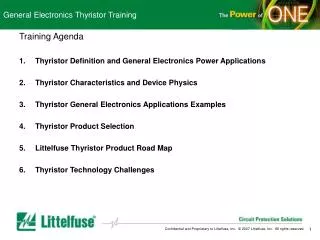
General Electronics TVS Diode Training Training Agenda • TVS Diode Definition and General Electronics Applications • TVS Diode Characteristics and Device Physics • TVS Diode General Electronics Application Examples • TVS Diode Product Selection • Littelfuse TVS Diode Product Road Map • TVS Diode Technology Challenges
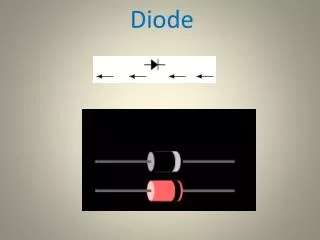
General Electronics TVS Diode Training • TVS Diode Definition Section 1 TVS Diode Definition and General Electronics Applications • TVS: Transient Voltage Suppressor • A TVS Diode is a clamping device that limits transient voltage spikes through a low impedance avalanche breakdown of a rugged silicon PN junction. • TVS Diodes are used to protect sensitive components from electrical overstress such as those induced by lighting strikes, inductive load switching, and Electro-Static Discharge (ESD). • TVS Diode Advantages in Circuit Protection Applications • Extensive range meeting industry requirements from 400 W to 10 kA • Exhibit excellent clamping ratio • Fast turn-on response: 1-5 ns • No inherent wear-out mechanism
TVS Diode Definition and General Electronics Applications Circuit Protection Needs in General Electronics Systems • A sudden change in the electrical condition of any circuit can cause a transient voltage to be generated from the energy stored in its inductance and capacitance. The rate of change in current in an inductor will generate a switching induced transient voltage. • Energizing the transformer primary • When a transformer is energized at the peak of the supply voltage, the coupling of this voltage step function to the stray capacitance and inductance of the secondary winding can generate an oscillatory transient voltage with a peak amplitude up to twice the normal peak secondary voltage. • De-Energizing the transformer primary • The opening of the primary circuit of a transformer generates extreme voltage transients. Transients in excess of ten times normal voltage have been observed across power semiconductors when this type of switching occurs. • Fault with inductive power source • If a short develops on any power system, devices parallel to the load may be destroyed as the fuse clears. • Switch Arcing • When current in an inductive circuit is interrupted by a contactor, the inductance tries to maintain its current by charging the stray capacitance.
TVS Diode Definition and General Electronics Applications • Typical TVS Circuit Protection Method - The device is used in reverse breakdown direction. - The device turns on when transient voltage exceeds VBR (Reverse Breakdown Voltage). - The device remains in a high-impedance off state while the voltage is below VBR.
TVS Diode Definition and General Electronics Applications Typical Discrete TVS Diode Packages for Circuit Protection
TVS Diode Characteristics and Device Physics Section 2 TVS Diode Characteristics and Device Physics Unidirectional TVS Diode IV Curve Unidirectional TVS Diode Characteristics V out V in For a Unidirectional TVS diode, the anode of the device should be grounded while the cathode connected directly to the line to be protected. When a positive surge is applied to the circuitry, the TVS diode is turned on (the reverse avalanche state). The output voltage level is determined by the VC specification of the TVS diode (ranges from 3 to 200 volts). When a negative surge is applied to the circuitry, the TVS diode turned on (the positive conducting state of the PN junction). The output voltage level is determined by the forward biasing voltage of the PN junction (ranges from 0.7 to 2 Volts). VC(Clamping Voltage) Voltage across the TVS diode at the IPP (peak pulse current) VBR (Reverse Break Down Voltage) Voltage at which the TVS diode turns on (conducting state) VRWM (Reverse Standoff Voltage) Voltage at which the TVS diode turns off (high impedance state)
TVS Diode Characteristics and Device Physics Bidirectional TVS Diode IV Curve Bidirectional TVS Diode Characteristics V in V out For a Bidirectional TVS diode, the device can be connected to the line to be protected symmetrically. When a positive or negative surge is applied to the circuitry, the TVS diode turns on (reverse avalanche state) in that direction. The output voltage level (ranges from 3 to 200 volts) is determined by the VC specification of the TVS diode in the respective direction of the voltage surge. VC(Clamping Voltage) Voltage across the TVS diode at the Ipp (peak pulse current) VBR (Reverse Break Down Voltage) TVS diode start to be at conducting state VRWM (Reverse Standoff Voltage) TVS diode start to be at high impedance state
TVS Diode Characteristics and Device Physics TVS Diode Electrical Characteristics Maximum Peak Pulse Power (PPPM ) Maximum Peak Pulse Power is the non- repetitive power dissipated in the TVS diode for a specific pulse. PPP ( Peak Pulse Power) = VC ( Clamping Voltage)x IPP ( Peak Pulse Current) Peak Pulse Power Testing Waveform The Maximum Peak Pulse Power is defined by applying a double exponential current waveform to the TVS diode. The typical wave shape used for testing are 8x20s and 10x1000 s waveforms.
TVS Diode Characteristics and Device Physics TVS Diode Thermal and Junction Capacitance Characteristics Peak Pulse Power De-rating Curve A TVS diode generates more heat for a given current pulse at higher ambient temperature. It also dissipates less heat at higher ambient temperatures. The maximum peak pulse rating is de-rated in proportion to the increase of ambient temperature. Junction Capacitance Characteristics The Capacitance of the TVS diode is due to the PN junction capacitance. PN junction capacitance is in indirectly proportional to the biasing voltage. The junction capacitance curve is linear at lower reverse biasing voltages.
TVS Diode Characteristics and Device Physics TVS Diode Construction Cross section of surface mount type Cross section of axial lead type
TVS Diode General Electronics Applications Examples Section 3 TVS Diode Applications Examples D.C. Supply Protection D.C. Line Protection A.C. Supply Protection EMI Limiting Single Line Relay and Contactor Transient Limiting
TVS Diode General Electronics Applications Examples TVS Diode Applications Examples Operational Amplifier (OpAmp) Microprocessor Data Bus Input Power Lines of Microprocessor
TVS Diode General Electronics Applications Examples Global Lab Capabilities • Qualification of all LF products • UL-Approved Customer Testing in ISO 17025 Lab (Des Plaines) • High power (AC/DC up to 1KV/50KA) UL approvals available in DP • Telcordia approvals in DP planned (2008) • Verification of Telcordia, ITU, IEC, FCC, and other industry, regulatory, and safety standards • Verification to various OC and OV standards • Insure application meets standards before submitting for approval • Customer Application testing • Assistance with design-in and performance verification • Help with selection of appropriate technology and rating • Application troubleshooting • Assistance insuring proper OV/OC and primary/secondary protection coordination • Competitive evaluations • Competitive or technology performance comparisons • Reliability & Tin Whisker data/testing
General Electronics TVS Diode Training Section 4 TVS Diode Product Selection • Matching the VRWM of the TVS diode with Normal Circuit Operation • Determine the reverse standoff voltage of the TVS: this must be larger than the normal operating voltage of the circuit. • Matching the PPPM with the Transient Voltage Threat from the Field • Determine the maximum peak pulse powerof the TVS diode: this must exceed that of the surge threat it is protecting. • The surge power of the threat is usually specified in regulatory requirements and standards such as IEC61000-4-5, GR 1089, etc. • Matching the VC with the Circuit Protection Needs • Determine the clamping voltage of the TVS diode: this must be lower than the respective voltage withstanding capability of the circuitry it is to protect. • Minimize the parasitic inductance cause by excessive board trace and lead length for ESD protection. • Matching the Signal Integrity Specifications • Determine and select the proper capacitance for high speed applications. • Determine the best board layout for impedance matching. • Application Testingis Always Helpful and May Be Necessary for Proper Selection • LF Global Labs provide extensive testing resources and application, regulatory, safety, and standards expertise for customer applications.
TVS Diode Product Selection Transient Voltage Suppression Devices Comparison Chart
TVS Diode Product Selection Typical TVS Diode Part Number Assignment Chart
TVS Diode Product Selection Special TVS Diode Part Number Assignment Chart
General Electronics TVS Diode Training Pb Free Product Section 5 Littelfuse TVS Diode Product Road Map
General Electronics TVS Diode Training Note: Primary focus is Automotive. Will look at differentiated opportunities in commodity products as they arise
General Electronics TVS Diode Training Section 6 General Electronics TVS Diode Technology Challenges • Higher Surge Ratings in Smaller Packages • Multiple Devices in a Single Package • TVS Diode Technology Combined With Other Technologies in the Same Package • Improved De-rating Characteristics • Higher Operating Temperatures