Download
1 / 3
490 likes | 2.64k Views
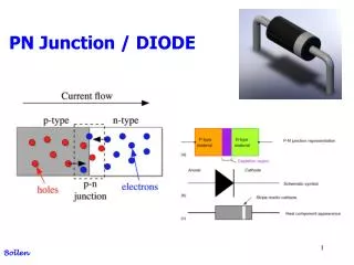
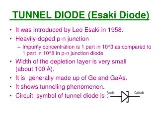
TUNNEL DIODE (Esaki Diode). It was introduced by Leo Esaki in 1958. Heavily-doped p-n junction Impurity concentration is 1 part in 10^3 as compared to 1 part in 10^8 in p-n junction diode Width of the depletion layer is very small (about 100 A). It is generally made up of Ge and GaAs.

E N D
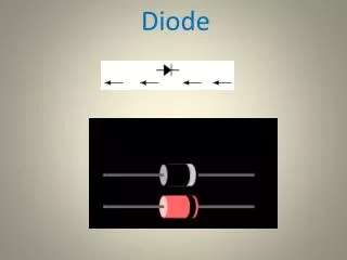
TUNNEL DIODE (Esaki Diode) It was introduced by Leo Esaki in 1958. Heavily-doped p-n junction Impurity concentration is 1 part in 10^3 as compared to 1 part in 10^8 in p-n junction diode Width of the depletion layer is very small(about 100 A). It is generally made up of Ge and GaAs. It shows tunneling phenomenon. Circuit symbol of tunnel diode is : EV
WHAT IS TUNNELING Classically, carrier must have energy at least equal to potential-barrier height to cross the junction . But according to Quantum mechanics there is finite probability that it can penetrate through the barrier for a thin width. This phenomenon is called tunneling and hence the Esaki Diode is know as Tunnel Diode.