Combinational Circuit Design and Simulation Using NAND Gates for BCD Decoder
This document presents the logical expressions and design for a combinational circuit, focusing on a 2421 to BCD decoder using NAND gates. It outlines the logic equations for various outputs and provides representations for each part of the circuit. Additionally, we explore the implementation of NAND gates with the SN74 series, including single and multiple input configurations. This comprehensive guide covers both theoretical and practical aspects, ensuring a clear understanding of digital circuits and their simulation.

Combinational Circuit Design and Simulation Using NAND Gates for BCD Decoder
E N D
Presentation Transcript
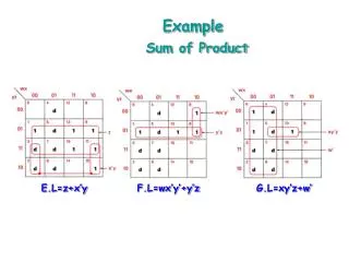
Example Sum of Product E.L=z+x’y F.L=wx’y’+y’z G.L=xy’z+w’
Example 4 Logic Diagram for 2421 to BCD Decoder A.L=w’z+x’yz’ B.L=xy’z’+x’yz C.L=wx’y’z’ D.L=xy’z+w’z+x’yz’ E.L=z+x’y F.L=wx’y’+y’z G.L=xy’z+w’
Combinational Circuit Design and Simulation Using Gates Introduction to Digital Integrated Circuits • SN74ALS00 • 4 two input NAND Gates Package • SN74ALS10 • 3 triple input NAND Gate Package • SN74ALS20 • Dual four input NAND Gate Package
Combinational Circuit Design and Simulation Using Gates 2 Input NAND GATE