Download
1 / 8
80 likes | 104 Views
CP/JEP backplane test module. What’s the maximum data rate into the S-CMM for phase-1 upgrade ?. CP / JEP backplane. JEMs and CPMs were designed to support 40Mb/s source terminated 2.5V CMOS signalling over full backplane length into high impedance CMM inputs

E N D
CP/JEP backplane test module What’s the maximum data rate into the S-CMM for phase-1 upgrade?
CP / JEP backplane JEMs and CPMs were designed to support 40Mb/s source terminated 2.5V CMOS signalling over full backplane length into high impedance CMM inputs • CPM : CMOS drivers, discrete resistors • JEM : FPGA outputs routed to backplane directly, on-chip “DCI” termination employed in current scheme Due to different implementation, the possible future increase in signalling rate might be different and might be achieved with different techniques. • JEMs are able to source low impedance, low voltage signals • JEM series termination is less than perfect (ringing) • CPM should exhibit better impedance match
JEM Backplane signals JEM scope shots: * series termination 160 Mb/s parallel termination 320Mb/s * Longest backplane tracks, noise generated on CMM and VME lines Conclusion: when operating JEMs at 160Mb/s and above, parallel termination on CMM should be employed
bandwidth Each CPM or JEM is sourcing a total of 50 lines into two mergers total capacity per module into both mergers is : 50 bit @ 40 Mb/s (25 bit of jet data) 100 bit @ 80 Mb/s (75 bit of jet data) * 200 bit @ 160 Mb/s (175 bit of jet data) * 400 bit @ 320 Mb/s (375 bit of jet data) * * On the JEMs, if we do not need to increase energy sum data volume, any increase on both backplane links can be used for jet data, if the increase in latency on the jet-to-sum processor path is acceptable (requires re-work of current jet processor DAQ interface)
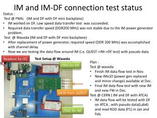
Rate tests • We’ve seen scope shots giving a rough indication of possible rate limits ~160 – 320 Mb/s on JEMs • We need to understand what the required bandwidth will be on CP and JEP • We will need to do bit error rate tests on backplane data with a module able to • terminate the signals for data rates ≥ 160Mb/s • deskew each signal line individually. Current CMMs could possibly be configured with BERT code at higher rates but will lack both termination at track impedance and fine grain deskew circuitry Build backplane tester based on recent FPGA family providing both termination and deskew
Backplane tester module • 9U module • Multi layer PCB with controlled impedance tracks • Single FPGA : Virtex-5 • per-pin deskew to < 80ps accuracy • “DCI” internal parallel termination • Covering all 400 merger input lines • Regional clocks for source synchronous transmission (clock forwarding) • Variable Vcco supply voltage to allow for various signal standards • External parallel termination to a subset of signal lines, in case DCI termination generates excessive power dissipation (up to ~ 15W) • Interface to • TTC clock (jitter attenuation required?) • VME -- • ??
The module... Auxiliary logic Backplane connector FPGA surrounded by terminators Bypass capacitors as needed, PCB bottom FPGA Add circuitry to be tried out for phase 1 / phase 2 ? regulators
... Start detailed design NOW