Download
1 / 32
320 likes | 445 Views
CLIC Advisory ComittEe,. Low emittance generation in Damping rings: Optics, DR layout, SC wigglers vs NC wigglers. Yannis PAPAPHILIPPOU. February 3 rd , 2010. DR parameters and challenges. High-bunch density

E N D
CLIC Advisory ComittEe, Low emittance generation in Damping rings: Optics, DR layout, SC wigglers vs NC wigglers Yannis PAPAPHILIPPOU February 3rd, 2010
DR parameters and challenges • High-bunch density • Emittance dominated by Intrabeam Scattering, driving energy, lattice, wiggler technology choice and alignment tolerances • Electron cloud in e+ ring imposes chamber coatings and efficient photon absorption • Fast Ion Instability in the e- ring necessitates low vacuum pressure • Space charge sets energy, circumference limits • Repetition rate and bunch structure • Fast damping achieved with wigglers • RF frequency reduction considered due to many challenges @ 2GHz (power source, high peak and average current) • Output emittance stability • Tight jitter tolerance driving kicker technology • Positron beam dimensions from source • Pre-damping ring challenges (energy acceptance, dynamic aperture) solved with lattice design
Schematic layout e- Damping Ring e- Pre-damping Ring e+ Pre-damping Ring e+ Damping Ring ACE 2010
Damping ring energy • Scaling of emittances with energy obtained with analytical arguments and including IBS effect (constant longitudinal emittance) • Broad minimum for horizontal emittance ~2-3GeV • Higher energy reduces ratio between zero current and IBS dominated emittance • Vertical emittance increases linearly with energy • Similar results obtained for other machines (e.g. CESRTA) • Choice of 2.86GeV in order to relax collective effects while achieving target emittances
PDR design F. Antoniou, CLIC09 Main challenge: Large input emittances especially for positrons to be damped by several orders of magnitude Design optimization following analytical parameterization of TME cells Detuning factor (achieved emittance/TME)> 2 needed for minimum chromaticity Target emittance reached with the help of conventional high-field wigglers (PETRA3) Non linear optimization based on phase advance scan (minimization of resonance driving terms and tune-shift with amplitude)
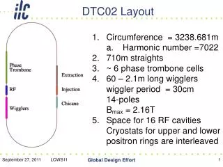
S. Sinyatkin, et al., LER 2010 DR layout • Racetrack shape with • 96 TME arc cells (4 half cells for dispersion suppression) • 38 Damping wiggler FODO cells in the long straight sections (LSS) • Space reserved upstream the LSS for injection/extraction elements and RF cavities ACE 2010
Arc cell S. Sinyatkin, et al., LER 2010 • 2.36m-long TME cell with bends including small gradient (as in NLC DR and ATF) • Phase advances of 0.452/0.056 and chromaticities of -1.5/-0.5 • IBS growth rates reduced due to optics function inversion ACE 2010
Wiggler cell and LSS S. Sinyatkin, et al., EPAC 2009 • LSS filed with wiggler FODO cells of around ~6m • Horizontal phase advance optimised for minimizing emittance with IBS, vertical phase advance optimised for aperture • Drifts of 0.6m downstream of the wigglers, long enough for absorbers, vacuum equipment and instrumentation ACE 2010
Dynamic aperture Horizontal Vertical New • Arc cell phase advance scan to optimize horizontal and vertical DA • Very large in both planes especially in vertical • Further optimisation DA needed (including misalignments, magnetic errors and wiggler effects) ACE 2010
New DR parameters • Reasonable magnet strengths (magnet models already studied) and space constraints • DA significantly increased • TME optics with gradient in the bend and energy increase reduces IBS growth factor to1.7(as compared to 5.4 in original DR design) • Further optics optimization with respect to IBS (F. Antoniou PhD thesis) and tracking code for comparaison with analytical theory ACE 2010
IBS tracking code A. Vivoli, LER2010 • Developed Monte-Carlo tracking code for IBS including synchrotron radiation damping and quantum excitation (SIRE, based on MOCAC) • Differences between analytical growth rates and the mean values obtained by 50 SIRE runs (under investigation) • Final emittances obtained by SIRE are just within the CLIC DR budget ACE 2010
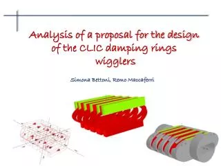
Wigglers’ effect with IBS Stronger wiggler fields and shorter wavelengths necessary to reach target emittance due to strong IBS effect Current density can be increased by different conductor type Nb3Sn can sustain higher heat load (potentially 10 times higher than NbTi) Two wiggler prototypes 2.5T, 5cm period, built and currently tested by BINP 2.8T,4cm period, designed by CERN/Un. Karlsruhe Mock-ups built and magnetically tested Prototypes to be installed in a storage ring (ANKA, CESR-TA, ATF) for beam measurements BINP PM wiggler NbTi SC wiggler Nb3Sn SC wiggler
Permanent magnet performance • Pure permanent magnet not able to reach very high field (i.e. 1.2T for Sm2Co17) • Pole concentrators used (e.g. vanadium permendur) to enhance pole field to a max value of 2.3T • Not more than 1.1T reached for 40mm period and 14mm gap • Higher field of 1.8T reached for 100mm period • Max field of 2.3T can be reached for a gap/period ratio of ~0.1, (140mm period for 14mm gap) • In that case, output emittance gets more than doubled (>800nm) • In order to reach target DR performance, number of wigglers has to be increased by more than a factor of 2, i.e. ~40% of ring circumference increase • Only way to reach high field for high gap/period ratio is by using super-conducting wigglers Simulations by P. Vobly Scaling by Halbach
Wiggler short prototypes CERN BINP Corrector coils with individual PS Regular coil Iron yoke End coils to compensate the first and the second integral ACE 2010
BINP NbTi Wiggler • Present design uses NbTi wet wire in separate poles clamped together • Wire wound and impregnated with resin and prototype assembled including corrector coil and quench protection system by spring 2009 • Field measurements in June showing poor performance (reaching 420 instead of 660A) due to mechanical stability problems (GFP separators) • Magnet delivered at CERN for further measurements and verification • New design under evaluation by BINP and CERN magnet experts
CERN prototype with NbTi wire 50 mm period 40 mm period • Crash test program at CERN with 40mm mock-up using NbTi wire • Reached peak field of 2.5T at 1.9K (2T at 4.2K) • Current density extrapolated to 50mm, provides more than 2.5T field • Currently continuing with Nb3Sn winding tests ACE 2010
Synchrotron radiation • Synchrotron radiation power from bending magnets and wigglers • Critical energy for dipoles and wigglers • Radiation opening angle • 90% of radiation power coming from the 76 SC wigglers • Design of an absorption system is necessary and critical to protect machine components and wigglers against quench • Radiation absorption equally important for PDR (but less critical, i.e. similar to light sources) ACE 2010
Radiation absorption scheme A 4-wigglers scheme • Gap of 13mm (10W/m) • Combination of collimators and absorbers • Terminal absorber at the end of the straight section (10kW) K. Zolotarev, CLIC09
Electron cloud in the e+ DR imposes limits in PEY (99.9% of synchrotron radiation absorbed in the wigglers) and SEY (below 1.3) Cured with special chamber coatings Fast ion instability in e- DR, molecules with A>13 will be trapped (constrains vacuum pressure to around 0.1nTorr) Other collective effects in DR Space charge (large vertical tune spread of 0.19 and 10% emittance growth) Single bunch instabilities avoided with smooth impedance design (a few Ohms in longitudinal and MOhms in transverse are acceptable for stability) Resistive wall coupled bunch controlled with feedback (100s of turns rise time) Collective effects in the DR G. Rumolo ρwig = 5x10¹²m-3, ρdip = 3x10¹¹ m-3 ACE 2010
Coatings for e- Cloud Mitigation M. Taborelli LER2010 • Bakeable system • NEG gives SEY<1.3 for baking @ > 180C • Evolution after many venting cycles should be studied • NEG provides pumping • Conceivable to develop a coating with lower activation T • Non-bakeable system • a-C coating provides SEY< 1 (2h air exposure), SEY<1.3 (1week air exposure) • After 2 months exposure in the SPS vacuum or 15 days air exposure no increase of e-cloud activity • Pump-down curves are as good as for stainless steel • No particles and peel-off • Very good results obtained at CESR-TA (although contaminated by silicon from kapton adhesive tape) bare Al CESRTA e+ TiN TiN new a-C CERN
RF system • RF frequency of 2GHz • R&D needed for power source • High peak and average power of 6.6 and 0.6MW • Strong beam loading transient effects • Beam power of 6.6MW during 156 ns, no beam during other 1488 ns • Small stored energy at 2 GHz • Wake-fields and HOM damping should be considered • 1GHz frequency considered (2 trains with 1ns bunch spacing) • Easier extrapolation from existing designs (e.g. NLC) • Lowering peak current and thus transient beam loading • Delay line for train recombination A. Grudiev, CLIC08
M. Barnes CLIC09 Kicker stability • Kicker jitter translated in beam jitter in IP, withσjit ≤0.1σx • Tolerance typically ~10-4 • Double kicker system relaxes requirement, i.e. ~3.3 reduction achieved @ATF • Striplines required for achieving low longitudinal coupling impedance • Significant R&D needed for PFL (or alternative), switch, transmission cable, feedthroughs, stripline, terminator (PhD thesis student at CERN) • Should profit from collaborator with ILC and light source community ACE 2010
Low emittance tuning M. Boege,, LER2010 • Present tolerances not far away from ones achieved in actual storage rings • SLS achieved 2.8pm emittance • DIAMOND claim 2.2pm and ASP quoting 1-2pm (pending direct beam size measurements) • Participate in low emittance tuning measurements in light sources (SLS) and CESR-TA ACE 2010
Emittances @ 500GeV • Light sources (SLS, DIAMOND and ASP) achieve ~2pm geometrical vertical emittance, at 3GeV, corresponding to ~12nm ofnormalised emittance • Below 2pm, necessitates challenging alignment tolerances and low emittance tuning • Seems a “safe” target vertical emittance for CLIC damping rings @ 500GeV • Horizontal emittance of 2.4µm is scaled from NSLSII parameters, a future light source ring with wiggler dominated emittance and 10% increase due to IBS
Route to 3TeV • The 3TeV design can be relaxed by including only a few super-conducting wigglers and relaxing the arc cell optics (reduce horizontal phase advance) • Another option may be operating a larger number of super-conducting wigglers at lower field of around 2T. • The same route can be followed from conservative to nominal design, considering that some time will be needed for low-emittance tuning (reducing the vertical emittance) • Considering the same performance in the pre-damping rings, the 500GeV design relaxes the kicker stability requirements by more than a factor of 2 • The dynamic aperture of the DR should be also more comfortable due to the relaxed arc cell optics • Energy loss/turn is significantly reduced and thereby the total RF voltage needed
CLIC/ILC DR collaboration • ILC and CLIC DR differ substantially as they are driven by quite different main RF parameters • Intense interaction between ILC/CLIC in the community working on the DR crucial issues: ultra low emittance and e--cloud mitigation. • Common working group initiated at the end of 2008 • Short term working plan includes • Chamber coatings and e--cloud measurements at CESRTA, • e-cloud and instability simulations with HEADTAIL (CERN) and CMAD (SLAC) • IBS measurements at CESRTA • Low Emittance Rings workshop organization (12-15/01/2010 @CERN) ACE 2010
LER2010 scope • Bring together experts from the scientific communities working on low emittance lepton rings (including damping rings, test facilities for linear colliders, B-factories and electron storage rings) in order to discuss common beam dynamics and technical issues. • Targets strengthening the collaboration within the two damping ring design teams and with the rest of the community. • Profit from the experience of colleagues who have designed, commissioned and operated lepton ring colliders and synchrotron light sources. ACE 2010
Beyond LER2010 • Low emittance rings working groups • Any other subjects? • Coordinators to be confirmed (others to be added?) • Task: Identify collaboration items as discussed in the workshop • Collect “expressions of interest” from community (LER2010 participants and beyond) • Start collaboration work to be reported to the next workshop! ACE 2010
Summary • PDR optics design achieves comfortable DA and energy acceptance • DR lattice design rationalised for space and magnet requirements, achieving large DA • Some refinement in non-linear dynamics needed for the CDR • IBS effect significantly reduced (energy increase, lattice design) • Monte-Carlo tracking simulations give encouraging results • DR performance based on super-conducting wigglers • Short prototype on “conventional” wire technology achieved required field • More challenging wire technologies and wiggler designs are under study • Robust absorption scheme • Collective effects (e-cloud, FII) remain major performance challenge • Novel coatings very promising as measurements in CESR-TA confirm low SEY • RF system present difficulties with respect to transients and power source at 2GHz • 1GHz frequency under consideration, including design of delay loop for train recombination • Stability of kickers challenging • Collaboration with ILC and light sources for technical design • Vertical emittance close to the ones achieved in modern light source • Participation in low emittance tuning measurement campaigns in SLS and CESR-TA • Working group on CLIC/ILC common issues for DR • Low Emittance Rings task groups established for expanding the collaboration • Established conservative and nominal DR parameters for CLIC @ 500GeV • Scaled design not far from existing design of existing or future light sources
R. Bartolini, LER2010 Brilliance and low emittance The brilliance of the photon beam is determined (mostly) by the electron beam emittance that defines the source size and divergence
R. Bartolini, LER2010 Comparison model/machine for linear optics * best achieved
R. Bartolini, LER2010 Vertical Emittance in 3rd generation light sources Best achieved values – not operational values Assuming 10–3 coupling correction , the V emittance of the new projects can reach the fundamental limit given by the radiation opening angle; Measurements of such small beam size is challenging !