Download

1 / 16
160 likes | 179 Views
Learn to implement Half Adder, Full Adder, 4-bit Ripple Carry Adder, and 4-bit Comparator using VHDL. Explore structured design techniques and apply them to complex circuits. Includes practical examples and concurrent statements.

E N D
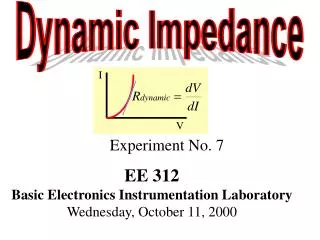
Experiment 7 Design of Binary Arithmetic Circuits
Experiment 6 Overview: • The Point: you used some relatively simple VHDL models to implement some relatively complicated circuits. • Include block diagrams • Concurrency = Concurrency (CSA) • VHDL code should look perfect • Properly indentation • Commented • Title banner (names, description, etc) • No line wrap! • Self commented names
Instructional Objectives: • To use concurrent VHDL statements in the design of arithmetic circuits • To design a Half Adder, Full Adder, 4-bit Ripple Carry Adder, and 4-bit Comparator
7-Seg Decoder Priority Encoder B3 B2 AA-AG B1 CATH B0 I7 I6 I5 Y2 I4 Y1 I3 Y0 I2 I1 STROBE I0 Connect to ground 4 switches (sensors) Alarm Control Break-in Armed OFF/ON_L Alarm Key Comparator I3 EQ I2 I1 I0 4 switches (access code) Digital Alarm System Experiment 7 P3
Binary Addition Given two 4-bit numbers, their sum A+B is calculated as follows a3 a2 a1 a0 + b3 b2 b1 b0 s3 s2 s1 s0 c2 c1 c0 cout
Half Adder A device, called a Half Adder, can be design to add a0+b0 in the least significant stage of the addition problem. Inputs: ai, bi Output: ci, si Obtain equations for ci and si from the truth table for the half adder.
Full Adder A device, called a Full Adder, can be design to add ai+bi, for i>0 stages of the addition problem. Inputs: ai, bi, ci-1(carry in to that stage) Output: ci, si Obtain equations for ci and si from the truth table for the full adder.
4-Bit Ripple Carry Adder Use one Half Adder (for the least significant stage) and three Full Adders. Propagate the carry through the circuit: ripple How many gate propagation delays before the carry out is valid?
4-Bit Comparator Given two 4-bit binary numbers, A and B, determine if they are equal. Multiple solutions: • Subtract B from A and test for zero result • Use XOR gates to do a bitwise comparison
VHDL Concurrent StatementRefresher ARCHITECTURE mad_hatter OF myhalfadder IS BEGIN concurrent statement1; -- half adder sum equation concurrent statement2; -- half adder carry equation END myarch;
VHDL Structural Modeling • Reflects modern digital circuit design • Supports readability, understandability, reuse of code • Supports preferred digital design approach: hierarchical design • Allows for the use of library-based modules • Allows for easy scalability of design • Utilizes software design techniques • Xilinx schematic capture software not reliable
VHDL Structural Modeling Similar to higher level language programming Example circuit
XCRPlus Development Board Carry out 4-bit sum Of A+B A B
Experiment 7 Overview P1: Design, test, and implement a Half Adder P2: Design, test, and implement a Full Adder P3: Design and implement a 4-bit Ripple Carry Adder Using Structural Modeling (Modelsim printout) P4: Design and implement a 4-bit Comparator Save for use in Experiment 9