Level 1 trigger sorter implemented in hardware
90 likes | 202 Views
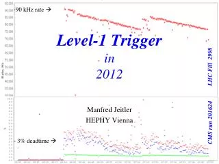
This document presents a comprehensive overview of the Level 1 Trigger Sorter implemented in hardware, detailing its architecture and functionality developed by Grzegorz Kasprowicz. It describes the two levels of high-rate triggers and the critical roles of various components, including the Event Building, Data Buffers, and Ethernet Mezzanine Board in the LHCb readout architecture. Key functions such as event sorting, error detection, and control signal generation are covered. The implementation achieves sorting speeds of around 4 million events per second, offering significant improvements in cost, space, and energy efficiency compared to previous network processor-based systems.

Level 1 trigger sorter implemented in hardware
E N D
Presentation Transcript
Level 1 trigger sorter implemented in hardware Grzegorz Kasprowicz
SWITCH SWITCH SWITCH SORTER SWITCH L1 FE SFC SFC L1 FE L1 FE L1 FE L1 FE L1 FE SFC SFC SFC SFC L1 FE L0 FE L0 FE ECAL RICH OT ST L0 FE MUON VELO L0 FE L0 FE L0 FE L0 TRIGGER HCAL L0 FE CPU CPU CPU CPU CPU CPU CPU CPU CPU CPU CPU CPU CPU CPU CPU CPU CPU CPU CPU CPU CPU CPU CPU CPU READOUT NETWORK SWITCH SWITCH SWITCH SWITCH SWITCH SWITCH SWITCH STORAGE LHCb readout architecture Two levels of high-rate triggers Detector 40 MHz 1 MHz TFC SYSTEM Front-End electronics LHC CLK 40KHz Event building CPU farm Grzegorz Kasprowicz
Overview of the TFC architecture Grzegorz Kasprowicz
Function blocs and data flow of Readout Supervisor Q_L1 – trigger sorter block L1 DBUF - Data Buffer (SRAM) L0 ABUF - Accept Data Buffer (dual port SRAM) GbE RX – PM3386 chip based Gigabit Ethernet mezzanine board L1 LINK – TLK2501 – 1.6 GBPS transceiver Grzegorz Kasprowicz
L1 Trigger Sorter Tasks: • Generation of control signals and receiving data from Ethernet mezzanine board • Sorting triggers according to event id number • Generation of control signals and data for TLK2501 transceiver • Error detection – missing trigger, wrong event number range, timeout • Counting processed triggers • Generating long and short trigger broadcasts for Q_MP • Generating addresses and signals for Accept Trigger Buffer (L0) and L1 Data Buffer Grzegorz Kasprowicz
To FEE How does it work? L1 Data Buffer (RAM) 1.6 GBPS transmitter (L1 Link) BCLK D A T A A D D R DATA control control RFCLK Ethernet Mezzanine Board FPGA PLL L1DBUF memory interface L1 Link interface DATA 6x32bit FIFO L1 TRG GBE From Readout Network TIMER Event number comparator control To Q_MP module Accept TRG memory Interface DATA Accept TRG Buffer (DPRAM) RX State machine Error Detection TX state machine L0 DATA ADDR Control interface control Grzegorz Kasprowicz LBUS
Detailed description A RX state machine reads the L1 trigger decision packets from the GbE RX via a 32-bit 80 MHz bus. The state machine drops the ten 32-bit words of IP protocol and writes via FIFO the eight 32-bit words of L1 trigger data into the L1 DBUF using the Event ID as the address. A TX state machine compares the L0 Event ID of the incoming L1 triggers with the L0 Event ID of the next trigger to broadcast stored in the L0 Accept Buffer. Upon receiving the next L1 trigger to broadcast, the state machine prepares the broadcast frame, transmits it together with a broadcast request to the TTC broadcaster in the Q_MP module. The state machine also ensures that the L1 trigger accept broadcasts are spaced by a minimum of 20 ms and that the first L1 trigger reject broadcast after a L1 accept is transmitted after 900ns and otherwise at intervals of 400 ns. Grzegorz Kasprowicz
Simulations Grzegorz Kasprowicz
Summary • This version, (not device optimized , with some safety margins) allows to achieve speed of sorting about 4 milion events per second, which leaves some safe margin • It is much cheaper, takes much less place and consumes much less energy than previously used Network Processor based sorter, because needs only one FPGA + memory GbE Interface card and L0 link transceiver will be mounted on RS board anyway Grzegorz Kasprowicz