Data Compression Module (DCM)
Data Compression Module (DCM). Tong-Long Fu Laboratory of RF Photonics, Department of Physics National Cheng Kung University, Tainan, Taiwan. 1. Outline. Review Development Schedule DCM Design Status of Prototype model testing Summary. 2. Review (1). DCM -- Data Compression Module

Data Compression Module (DCM)
E N D
Presentation Transcript
Data Compression Module(DCM) Tong-Long Fu Laboratory of RF Photonics, Department of Physics National Cheng Kung University, Tainan, Taiwan 1
Outline • Review • Development Schedule • DCM Design • Status of Prototype model testing • Summary 2
Review (1) DCM -- Data Compression Module compress raw scientific data 3
Review (2) What has been done since SDR? • Select main parts of DCM • ADI DSP 21020 as the core DSP chip • Order development tools for key parts • Actel FPGA and ADI DSP 21010 • Collect software codes and test on PC (visual C++) • Prepare the interface specification documents • Start the design of DCM • make the board for functional tests (prototype model) 4
Development Schedule (2) Documents to be issued 6
DCM Design • DCM and its interface • Work flow, Mode action, and Memory Map • Parts information- power consumption and radiation tolerance • Clock, control lines, and BIOS functions • I/O control: CDI, SOH, and error handling • Interface to MM: format • Algorithms: compression and decompression 7
DCM Interface MM MMCB PLB data Functional Block Diagram 5V (TBD) mA DPU DSP PROM Max. 5W FPGA SRAM DCM DCM design 8
DCM Clock (Oscillator) DSP Data Memory (SRAM) Program Memory (SRAM) BIOS (PROM) • W/R • Memory Select Logic Device (FPGA) W/R DCM design 9
Work Flow DCM design 10
Mode Action Flow DCM design 11
DCM Schematic Diagram DPU Reset CDI_CLK • DCM • DSP • FPGA (Logic device) • SRAM (PM and DM) • PROM (BIOS) CDI_DCOE CDI_STB CDI_DAT(C) CDI_DAT(R) 16 bits Data Bus MM -MMCB -PLB 24~27 bits Address Bus DCM design 12
Internal Memory interface DCM design 13
Program Memory Data Memory 0x00 0000 0x00 0000 BIOS (PROM- pm_ban0) (Prototype model use EEPROM) MM (dm_bank0) 0x00 0200 Not use 0x80 0000 Program SRAM (SRAM- pm_ban1) 0x800 0000 Data Program Memory (dm_bank1) 0x82 0000 Not use 0x FFFF FFFF 0x FF FFFF compression memory map DCM design 14
Item Product Company Radiation hardness value note 1 DSP RH21020 Lockheed Martin 1Mrads TSC20102F TEMIC 100Krads 2 oscillator ? ? ? 3 FPGA RH1280 Actel 300Krads 4 SRAM HX6228 (128Kx8 bit) Honeywell 1Mrads 5 PROM R29793B/883B (8192x8 bit) Fairchild ? Standard US Mil-883/B 6 EEPROM 28c010TRP (128Kx8 bit) SpaceElectronics, Inc 50-250Krads Parts and Radiation tolerance DCM design 15
Power Consumption Item Parts Required power per unit unit Required power Note 1 DSP chip (Temic TSC21020F) <1.36 W (typical) 1 ~1.36 W lCan be estimated by formula lSee Temic datasheet 2 20 MHz Oscillator (Q-Tech.)(?) ? 1 ? 3 FPGA (Actel RH1280) ~1.44 W 1 ~1.44W lCan be estimated by formula lSee Actel datasheet 4 SRAM (Honywell HX6228; 128KX8) 0.5 W 6 3W lTypical operating power 25mW/MHz l5mW per unit for disable mode 5 PROM (Fairchild R29793SM/883B) 1.05W (enable mode) 2 2.1W 0.275W per unit (disable mode) * EEPROM (SpaceElectronics, Inc 28C010TRP) 0.4W 2 lIn MM lTypical operating power 20mW/MHz 0.8W DCM design 16
Clock and Control lines - Timing Specification: 1. Internal Clock (in DCM): 20MHz oscillator 2.Control Line : (defined at SDR) Action at Low level (duration 100 ms ) Action at Low level (duration 2us ) High level : Not Busy Busy Low level : Busy DCM design 17
Development chain Check CDI Working Modify Hardware FPGA Design Add I/O Subroutine I/O, Logic Device and Hardware CDI_Manpower DCM design 18
BIOS function I/O Code (BIOS) DSP-initialized Routine CDI Process Routine Self-Test Routine Data Transmission Routine I/O Data (BIOS) Data initialization Command Table DCM design 19
BIOS Work Flow DCM design 20
CDI Process DCM design 21
CDI and SOH Process (1) c7 c6 c5 c4 c3 c2 c1 c0 d15 d14 d13 d12 d11 d10 d9 d8 d7 d6 d5 d4 d3 d2 d1 d0 1. Signal Timing : (From CDI; defined by UCB) -Command Cycle CDI_CLK : 2M Hz CDI_DAT(C) : 8 bits Command ; 16 bits Information DCM design 22
CDI and SOH Process (2) -Readback Cycle CDI_CLK : 2M Hz CDI_DAT(C) : 8 bits Command CDI_DAT(R) : 16 bits Data DCM design 23
CDI and SOH Process (3) - Bits for Command Assignments (defined by CDI) - Current Command assignment for the commands in command cycle [20-3F] • Four functions of CDI command are assumed: • Inquiring certain state of the status of health • Debugging/ trouble-shooting • Backup support for control lines • Backup support for MM addressing DCM design 24
CDI commands (1) DCM design 25
CDI commands (2) DCM design 26
CDI commands (3) DCM design 27
CDI commands (4) DCM design 28
SOH- Status of Health (1) - Current command assignment for Readback Cycle DCM design 29
SOH[0:7] More message in SOH[8:15] 0: yes 1: no Repeat inquire command 32 kinds: [0-31] for [20-3F] Command executed 0: succeed 1: failed SOH[8:15] Report the details: 128 states SOH- Status of Health (2) E2 command (confirmation) Check sum [0:7] Check sum [8:15] DCM design 30
1: OK 0: Not 1: OK 0: Not 1: OK 0: Not 1: OK 0: Not 1: OK 0: Not 1: OK 0: Not 1: OK 0: Not 1: OK 0: Not SOH[0:7] PROM (ROM_1) PROM (ROM-2) SRAM (PM_1) SRAM (PM_2) SRAM (DM_1) SRAM (DM_2) SRAM (DM_3) SRAM (DM_4) 1: OK 0: Not 1: OK 0: Not 1: OK 0: Not 1: OK 0: Not 1: OK 0: Not SOH[8:15] 1: OK 0: Not 1: OK 0: Not DSP FPGA Power Read PLB DCM task Clock Read/Write MMCB SOH- Status of Health (3) E3 command (status through-out) Check sum [0:15] DCM design 31
Error Handling After receiving SOH from DCM, what DPU can help DCM, if there is some error ? • Send DCM_Reset Signal again. • Interrupt DCM work. • Cut-off some devices of DCM (e.g., PROM, SRAM…) • Add some advanced work through CDI . DCM design 32
MM Format (1) -MMCB: 7 byte 7 byte 1 byte MM OI CI Status Code -MMCB -PLB -Data • Information include: 1. Data type 2. Data Status 3. Check Bits 4. DCM Status -PLB: MM:Mass Memory MMCB: Mass Memory Control Block PLB : Program Loading Block OI : Original data Information CI : Compressed data Information Memory Map? (TBD) DCM design 33
MM Format (2) 1 byte - Data type • Data type Include : • Camera data - Sprite Burst mode (SBM) • Camera data – Sprite Continuous • Continuous mode (SCM) • Camera data – Aurora / Airglow mode (AAM) • Spectrophotometer data (SP) • Array Photometer data (AP) • (more may be added) OI CI • Start • Address 4 byte 2 byte - Data Size 1 byte - Data type • Start • Address 4 byte 2 byte - Data Size DCM design 34
Algorithm consideration (1) • More complicated operations and algorithms, more requirements/loads on hardware (SRAM, EEPROM, FPGA, and PROM) and power • Factors of trade-off • Code size – SRAM (Program memory) • Power • Algorithm complexity • Compression ratio DCM design 35
Code Size Estimate Some typical code sizes of data compression Testing with Visual C++ 6.0 DCM design 36
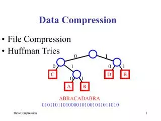
Codes for compression • Imager data • Large redundancy in space • A theoretical upper limit on compression ratio C~ 17 can be roughly estimated • Thus, new algorithm with large compression ratio should be developed • Data from array photometer (AP)/spectrometer (SP) • After trigger, wild variation in short duration • Still have some redundancy, but may be not so large, in time domain after transient • Common data compression algorithm should be enough Image coder Common coder DCM design 37
Proposed algorithms • Testing: ranger coder • Compression ratio C 2 • A universal encoder (no statistical table) • Code size in TI DSP C6x ~ 52 Kbyte (program memory) • Code size in ADI DSP not available yet • In development: • Wavelet coding with Huffman coding/decoding • One-dimensional algorithm is ready • Two-dimensional algorithm still needs to develop • Huffman coding (require statistical table) • Algorithm is ready • Arithmetic coding (require statistical table) • Algorithm is ready DCM design 38
Read MMCB Data type/data length Verify data type no no Imager data? Require Averaging? yes yes Select image coder Do Averaging Select common coder Setup verification (check sum) Build up header Compression Write MMCB header/compressed data Compression flow diagram DCM design 39
Compressed data • Header (compression information) • compressed raw data decompression verification Read header Build Statistical table Decoder selection Build raw data file with header (statistical table) Decode the compressed data Data file output Decompression flow chart Development platform: visual C++ DCM design 40
Prototype model testing (1)Parts list Parts used in the Prototype model development Model testing 41
Prototype model testing (2)DSP_Schematic Model testing 42
Prototype model testing (3)Data Memory Model testing 43
Prototype model testing (4)Program memory Model testing 44
Prototype model testing (5)Logic Device (FPGA) Model testing 45
Top view Bottom view Prototype model testing (6)DSP_Test Board PCB Model testing 46
(a) sample 1, 512 x 80, 165 Grays (b) sample 2, 512 x 80, 237 Grays (c) sample 3, 512 x 80, 237 Grays Two sample Picture (d) sample 4, 237 x 172, 30 Grays (e) sample 5, 237 x 172, 30 Grays Simulation: Range Coder Model testing 47
Summary • Some issues remain to be solved • DSP chip for the flight model • RH21020 or TSC21020F • Impact: speed and clock (25 MHz or 20 MHz), power • Input Scientific Data resolution • 8 bits, 16 bits or 12 bits? • Impact: code implementation; SRAM allocation • Solution: calculation based on IEEE 32bits floating point standard 48