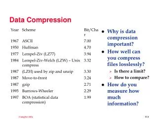
Data Compression Module ( DCM )
Data Compression Module ( DCM ). IFR Status Report. Tong-Long Fu Laboratory of RF-MW Photonics, Department of Physics National Cheng Kung University, Tainan, Taiwan. Review. Basic architecture set at PDR meeting At IFR ,Status of DCM Design Prototype model Testing


Data Compression Module ( DCM )
E N D
Presentation Transcript
Data Compression Module( DCM ) IFR Status Report Tong-Long Fu Laboratory of RF-MW Photonics, Department of Physics National Cheng Kung University, Tainan, Taiwan
Review • Basic architecture set at PDR meeting • At IFR ,Status of DCM • Design • Prototype model • Testing • DCM Characteristics • Will be presented …
Outline 1. Hardware /Software System Design and specification (1). Prototype Module . (2). Schematic Diagram. (3). FPGA Design (4). Specification and Testing Design Plan (5). Software Code Test (6). CDI Testing 2. DCM working and timing definition 3. DCM Hardware Limitation and Improvement 4. Conclusions and Future Works
Prototype Module (1) Layer Structure : - Top Level , - Middle Level , - Bottom Level DCM Prototype Testing Board : - includes “DSP Main Board” ,”Memory Board”,and “Logic Board” Purpose: 1. Easy to Test each part of board. 2. Easy to modify any part of board. 3. Easy to develop hardware system
Prototype Module (2) • DSP Main Board : Use ADSP 21020 (133 MHz) to test and support stable clock , stable power and JTAG testing port. • Memory Board : Use six IDT71024 SRAM and AT28C10 EEPROM to testing
Prototype Module (3) -Use ICE to test and load test code to DSP ICE can help us to debug DSP and load code . -DSP connect Memory board FPGA also connect after memory board .
Prototype Module (4)IC Replacement “?” should be provide UCB
Prototype Module (5)Tools and Devices * Need to order more for backup
Power On State initialized or Reset Signal - Test DSP (or sent reset signal to DSP) OK Auto test - FPGA interrupt DSP,when CDI information OK is sent to FPGA . Then FPGA send data to DSP - From Timing ,we can check detail action CDI Process FPGA working Flow
FPGA Performance and limitation - DCM System speed ~ 25MHz Now Used logic Some part we have not add it .include debug part ….
Simulation environment • Testing of Interface : • Simulate DPU Action • - DAQMIO-16B Card • Simulate CDI Information • - DAQDIO32HS Card • Code Testing • JTAG Testing Port
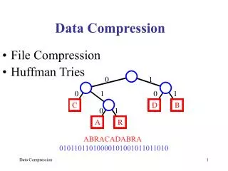
DCM - Software Sample Pictures 634X470 (256 Grays) Org Size: 293KB Some ideals we had discuss in the SDR and PDR . DCM-Software Code include : BIOS Code Program Code We need some typical sample picture of “aurora” and “airglow” to do more simulation .
Code Efficiency C. R. : Compression Rate
CDI Simulation (1) Command Cycle Timing Readback Cycle Timing • Using DIO32HS to simulate CDI Signal • Using external clock to get stable 2 MHz CDI_CLK
CDI Simulation (2) Using LabView to control DIO card , and simulating CDI signal for DCM . For testing environment of DCM ,we need create a DTE (DCM testing environment )
CDI Stimulation (3) DAQ has internal clock ~20 MHz, but it is not stable when using 2 MHz clock . Use external clock to get a stable signal .
DCM Interface Signal Timing (2)- Memory Bus for Write Memory Define at PDR : Access Time = ~ 200 ns
DCM Interface Signal Timing - CDI - Reference from UCB
Memory Size limitation DCM Module Memory : For DCM Memory Size now is follow limitation further ADSP. If size expansion is necessary ,we could modify FPGA code “?? ” need to specify by UCB
DCM Interface : Electric Characteristics for Design Reference • In the finial prototype testing , we will determent all the real testing condition. • we estimate its parameter to help us testing . • So It is just reference for our design . “?” need to settle by UCB and NCKU together
DCM System Specification “*?” Could you provide us some suggestions?
Connection Socket - Testing Socket : Maybe use 40 pins connector - Connection to MM : Reference from UCB - Connection to DPU : Reference from UCB
Direction of Improvement Improvement Key Point
Conclusions and Future Works • 1. Now I have finished: • CDI – Testing • The first version of Prototype module • Some Code Testings • Initial design architecture of DCM 2. The Furture Works • Due to contract problem ,so the work of DCM have been delayed . • Need to set regular schedule for interface review and technical discussion • Testing and design improvement . (Need to document) • Hope to get more testing information of AEP from UCB
Thanks Fu The End