Download
1 / 35
370 likes | 418 Views
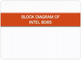
Learn about the Intel 8085 microprocessor introduced in 1976, its key features, advanced versions, block diagram, units like Processing Unit, Instruction Unit, and Storage Interface Unit, and components like Accumulator, ALU, Status Flags, PSW, and more.

E N D
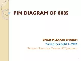
Introduction to 8085 • It was introduced in 1976 • It is 8-bit microprocessor. • Its actual name is 8085 A. • It is single NMOS device. • It contains 6200 transistors approx. • Its dimensions are 164 mm x 222 mm. • It is having 40 pins Dual-Inline-Package (DIP).
Introduction to 8085 • It has three advanced versions: • 8085 AH • 8085 AH2 • 8085 AH1 • These advanced versions are designed using HMOS technology.
Introduction to 8085 • The advanced versions consume 20% less power supply. • The clock frequencies of 8085 are: • 8085 A 3 MHz • 8085 AH 3 MHz • 8085 AH2 5 MHz • 8085 AH1 6 MHz
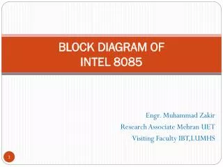
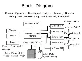
Three Units of 8085 • Processing Unit • Instruction Unit • Storage and Interface Unit
Processing Unit • Arithmetic and Logic Unit • Accumulator • Status Flags • Temporary Register
Instruction Unit • Instruction Register • Instruction Decoder • Timing and Control Unit
Storage and Interface Unit • General Purpose Registers • Stack Pointer • Program Counter • Increment/Decrement Register • Address Latch • Address/Data Latch
Three Other Units • Interrupt Controller • Serial I/O Controller • Power Supply
Accumulator • It the main register of microprocessor. • It is also called register ‘A’. • It is an 8-bit register. • It is used in the arithmetic and logic operations. • It always contains one of the operands on which arithmetic/logic has to be performed. • After the arithmetic/logic operation, the contents of accumulator are replaced by the result.
Arithmetic & Logic Unit (ALU) • It performs various arithmetic and logic operations. • The data is available in accumulator and temporary/general purpose registers. • Arithmetic Operations: • Addition, Subtraction, Increment, Decrement etc. • Logic Operations: • AND, OR, X-OR, Complement etc.
Temporary Register • It is an 8-bit register. • It is used to store temporary 8-bit operand from general purpose register. • It is also used to store intermediate results.
Status Flags • Status Flags are set of flip-flops which are used to check the status of Accumulator after the operation is performed.
Status Flags • S = Sign Flag • Z = Zero Flag • AC = Auxiliary Carry Flag • P = Parity Flag • CY = Carry Flag
Status Flags • Sign Flag (S): • It tells the sign of result stored in Accumulator after the operation is performed. • If result is –ve, sign flag is set (1). • If result is +ve, sign flag is reset (0).
Status Flags • Zero Flag (Z): • It tells whether the result stored in Accumulator is zero or not after the operation is performed. • If result is zero, zero flag is set (1). • If result is not zero, zero flag is reset (0).
Status Flags • Auxiliary Carry Flag (AC): • It is used in BCD operations. • When there is carry in BCD addition, we add 0110 (6) to the result. • If there is carry in BCD addition, auxiliary carry is set (1). • If there is no carry, auxiliary carry is reset (0).
Status Flags • Parity Flag (P): • It tells the parity of data stored in Accumulator. • If parity is even, parity flag is set (1). • If parity is odd, parity flag is reset (0).
Program Status Word (PSW) • The contents of Accumulator and Status Flags clubbed together is known as Program Status Word (PSW). • It is a 16-bit word.
Instruction Register • It is used to hold the current instruction which the microprocessor is about to execute. • It is an 8-bit register.
Instruction Decoder • It interprets the instruction stored in instruction register. • It generates various machine cycles depending upon the instruction. • The machine cycles are then given to the Timing and Control Unit.
Timing and Control Unit • It controls all the operations of microprocessor and peripheral devices. • Depending upon the machine cycles received from Instruction Decoder, it generates 12 control signals: • S0 and S1 (Status Signals). • ALE (Address Latch Enable).
Timing and Control Unit • RD (Read, active low). • WR (Write, active low). • IO/M (Input-Output/Memory). • READY • RESET IN • RESET OUT • CLK OUT • HOLD and HLDA
General Purpose Registers • There are 6 general purpose registers, namely B, C, D, E, H, L. • Each of the them is 8-bit register. • They are used to hold data and results. • To hold 16-bit data, combination of two 8-bit registers can be used. • This combination is known as Register Pair. • The valid register pairs are: • B – C, D – E, H – L.
Program Counter • It is used to hold the address of next instruction to be executed. • It is a 16-bit register. • The microprocessor increments the value of Program Counter after the execution of the current instruction, so that, it always points to the next instruction.
Stack Pointer • It holds the address of top most item in the stack. • It is also 16-bit register. • Any portion of memory can be used as stack.
Increment/Decrement Register • This register is used to increment or decrement the value of Stack Pointer. • During PUSH operation, the value of Stack Pointer is incremented. • During POP operation, the value of Stack Pointer is decremented.
Address Latch • It is group of 8 buffers. • The upper-byte of 16-bit address is stored in this latch. • And then it is made available to the peripheral devices.
Address/Data Latch • The lower-byte of address and 8-bit of data are multiplexed. • It holds either lower-byte of address or 8-bits of data. • This is decided by ALE (Address Latch Enable) signal. • If ALE = 1 then • Address/Data Latch contains lower-byte of address. • If ALE = 0 then • It contains 8-bit data.
Serial I/O Controller • It is used to convert serial data into parallel and parallel data into serial. • Microprocessor works with 8-bit parallel data. • Serial I/O devices works with serial transfer of data. • Therefore, this unit is the interface between microprocessor and serial I/O devices.
Interrupt Controller • It is used to handle the interrupts. • There are 5 interrupt signals in 8085: • TRAP • RST 7.5 • RST 6.5 • RST 5.5 • INTR
Interrupt Controller • Interrupt controller receives these interrupts according to their priority and applies them to the microprocessor. • There is one outgoing signal INTA which is called Interrupt Acknowledge.
Power Supply • This unit provides +5V power supply to the microprocessor. • The microprocessor needs +5V power supply for its operation.