Download
1 / 21
210 likes | 505 Views
Plasma CVD Carbon Nanotubes. Instructor: Yonhua Tzeng An-Jen Cheng April 19 2004. Questions. What is the major effect for growing carbon nanotubes by HFPECVD? Why can carbon nanotubes be bent by ion bombardment?. Introduction.

E N D
Plasma CVD Carbon Nanotubes Instructor: Yonhua Tzeng An-Jen Cheng April 19 2004
Questions • What is the major effect for growing carbon nanotubes by HFPECVD? • Why can carbon nanotubes be bent by ion bombardment?
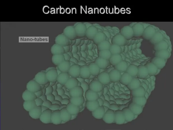
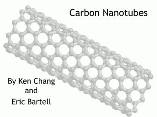
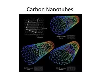
Introduction • Carbon nanotubes which have a hexagonal structure are synthesized in plasmas containing ionized carbon atoms, and carbon nanotubes can be divided into single- and multi-wall . • Carbon nanotubes can be synthesized by MW-PECVD, RF-PECVD, HF-PECVD, pyrolysis, laser evaporation and so on. • Carbon nanotubes exhibit semiconducting or metallic properties depending on their diameter and helicity of the arrangement of graphite rings in the wall. • Carbon nanotubes have preeminent electric, thermal, and mechanical properties such as high aspect ratio, high stress, high resistance to chemical and physics attack.
Outline • The effects and parameters of magnetron-type radio-frequency plasma for carbon nanotubes growth. • Growing carbon nanotubes by hot filament plasma enhanced chemical vapor deposition, and control carbon nanotubes’ shape by ion bombardment. • Effects of coating a ultrathin polymer films on carbon nanotubes by plasma treatment.
RF magnetron-type apparatus • 1. A powered Ni RF electrode is installed in the center of a grounded cylindrical chamber. • PECVD for nanotubes growth is performed under the conditions of 0.5 Torr and RF power of 1000W. • A magnetic field (0≤Bz≤340G) is externally applied parallel to the powered cylindrical RF electrode using solenoid coil in order to achieve lower plasma sheath voltage and higher plasma density. • The low-pass filter (LPF) is used to control the DC bias voltage component (V rf) and DC current density (J rf) toward the RF electrode. • Gas sources: Methane and hydrogen (9:1). Ref: G-H, Jeong, N. Satake, T. Kato, T. Hirata, R. Hatakeyama, K. Tohji, Jpn. J.Appl. Phys., 42 (2003), ppL1340-L1342
SEM images show the features of nucleation and successive nanotubes growth during PECVD with time evolution. (a) As polished Ni RF electrode surface (b) after sputtering for 15 min ( c) after 1 min growth using the mixture of CH4 and H2 (d) after 3 min growth (e) after 7 min (f) after 15min growth Ref: G-H, Jeong, N. Satake, T. Kato, T. Hirata, R. Hatakeyama, K. Tohji, Jpn. J. Appl. Phys., 42 (2003), ppL1340-L1342
Effects of magnetic field • 1.SEM images showing the effects of magnetic field externally introduced to the vacuum chamber. (a) Bz =0G, (b) Bz =170G,(c) Bz= 340G • Image (a) shows that when Bz= 0 and Vdc=-890V, most of the creations consist of amorphous carbon and graphite material. • The density of nanotubes grown in Bz= 170G and Vdc=-380V is higher than the result in the case of Bz= 340G and Vdc=-180V. • It is found that plasma confinement and self-bias control by magnetic field introduction have critical effects on the carbon nanotubes growth REF: T. Hirata, N. Satake, G.-H. Jeong, T. Kato, R. Hatakeyama, K. Motomiya, K.Tohji, Appl. Phys. Lett., 82, 1119, 2003
Effect of current density • SEM images showing the MWCNTs produced on the RF electrode under the condition of (a) Jdc=0mA/cm2 , Vdc=-180V (b) Jdc=1.5mA/cm2 , Vdc=-235V (c) Jdc=4.0mA/cm2 , Vdc=-570V,and (d) dependence of nanotubes density on Jdc. • The DC bias voltage of the RF electrode (Vdc) is externally changed for typical magnetic fields ( 170, 240, and 340G ) . An uniform, dense, and straight MWCNTs grow in the externally bias case of Jdc=1.5mA/cm2 , Vdc=-235V as shown in Fig. (b). • Carbon nanotubes are observed to grow along the local electric field due to the potential drop in the plasma sheath formed by Vdc. • DC bias voltage which directly determine the ion bombarding energy in the plasma sheath. • The typical parameters measured by Langmuir probe, such as Te=5eV, ne=5*1010cm-3, and φp=10V, the sheath thicknesses were found to be 3-6.7mm. REF: T. Hirata, N. Satake, G.-H. Jeong, T. Kato, R. Hatakeyama, K. Motomiya, K.Tohji, Appl. Phys. Lett., 82, 1119, 2003
(a) Variation of the nanotubes length with growth time and (b) diameter distribution of the MWCNTs grown for 3 min and 15min (c) TEM image of individual MWCNT, and (d) Raman spectrum of the uniformly grown MWCNTs. We found that the nanotubes growth rate in this study is 0.5μm/min, and the nanotubes diameter distribution becomes narrower; in other words, although MWCNTs grown at the early stage have various diameters but most of the MWCNTs after 15 min growth have similar diameter of 100-120nm Ref: G-H, Jeong, N. Satake, T. Kato, T. Hirata, R. Hatakeyama, K. Tohji, Jpn. J. Appl. Phys., 42 (2003), ppL1340-L1342
HFPECVD Carbon nanotubes growth • During deposition, the gas pressure of 10 Torr (50%C2H2 and 50 % NH3) was kept constant, and the temperature of the substrate was about 650°C. The power of the DC plasma was 160W (400V, 0.4A) and the time of deposition was 3 min. The distance between filament and substrate was about 5-10mm. • Acetylene(C2H2) and ammonia(NH3) gas were used as a carbon source and catalyst. • Prior to carbon nanotubes growth, the substrate was cleaned in acetone and methanol for 10 min. Fig. Schematic diagram of plasma enhanced hot filament chemical vapor deposition reactor REF: J.-H Han, W.-S. Yang, J.-B. Yoo, C-Y Park, J. Appl. Phys., 88, 7363, (2000) H. Lim, H. Jung, S.-K. Joo, Microelectronics engineering 69 (2003) 81-88
Effect of plasma density for nanotubes growth • The bias voltage for plasma decreased from 550 to 429V , the substrate temperature change from 580 to 530°C with decrease in the bias voltage. As shown in Fig.(a), the vertically aligned carbon nanotubes were grown at the plasma power of 550V and 0.15A. But as shown in Figs. (b) and (c), the growth of carbon nanotubes was not observed at plasma power lower than 550V(0.15A) • The filament current is expected to play important roles such as heating the substrate and electron generation. The fact that the growth of carbon nanotubes changes under the same filament current implies that plasma power plays a more important role than the filament current on carbon nanotubes growth. Fig. Effect of plasma power on the growth of carbon nanotubes at a constant filament current of 14 A: (a) 550V (0.15A) (b) 504V (0.11A) (c) 450V (0.06A) (d) 430V (0.02A)
Effect of plasma density for nanotubes growth • The plasma power and the filament current were simultaneously varied to maintain a constant substrate temperature (556°C) in the HFPECVD system. • As shown in Fig.1 (a)-(d), an increase in plasma power enabled the carbon nanotubes to be grown dramatically even though the filament current decreased. • The plasma power may be the most crucial factor for determining the growth characteristics of carbon nanotubes. • Without the filament current, the growth of vertically well-aligned carbon nanotubes was also observed and shown in Fig.2 (b) Fig.1.Effect of plasma power on the growth characteristics of carbon nanotubes at a constant temperature of 556°C: (a) 500V (0.13A) (plasma power),12.1A (filament current) (b) 551V (0.15A), 11.1A (c) 600V(0.21A,(A,(d) 650V (0.25A,7A Fig.2. SEM images of carbon nanotubes grown on Ni coated glass without filament current : (a) 650V (0.23A) , 25min (b) 640V (0.23A), 40 min REF: J.-H. Han, W.-S. Yang, and J.-B Yoo, C.-Y Park, J. Appl. Phys., 88, 7363 (2000)
Ion mass doping system Fig. Schematic of the ion mass doping system Fig. Two cases of CNTs specimens :(a) perpendicular, (b) at 45° to the ion shower REF: H. Lim, H. Jung, S.-K. Joo, Microelectronics Engineering 69 (2003) 81-88
Effect of Ion Bombardment • Ion bombardment was used to bend the carbon nanotubes structure, the shape of the CNTs did not change when the ion beam was perpendicular to the substrate; however, CNTs were bent when the CNTs was tilted to 45 degree. • The reasons for the CNTs to bend: 1.The unique features of the process in IMDS such as DC bias and physical etching. A strong electric field during the ion shower may be the reasons that cause the CNTs to bend. Fig. Carbon nanotubes after Ar ion bombardment (a) with substrate perpendicular to ion shower (b) at angle of 45°C REF: H. Lim, H. Jung, S-K. Joo, Microelectronics Engineering 69 (2003), 81-88
Cont. • After placing the carbon nanotubes tilted for an hour at the same electric field without ion bombardment, there is no trace to find out carbon nanotubes have been bent in such a high electric field. • The physical damage on the carbon nanotubes wall may be another reason. • The carbon nanotubes were damage on only one side of the wall and bent toward the etched side, being etched means that carbon nanotubes loses some carbon atoms. It reported that carbon nanotubes yield to plastic deformation under tensile stress. Fig. No change of carbon nanotubes after expose to electric field of 5 kV/cm without ion bombardment Fig. TEM image of asymmetrically etched carbon nanotubes REF: H. Lim, H. Jung, S-K. Joo, Microelectronics Engineering 69 (2003), 81-88
Polymer film coating • The carbon nanotubes were vigorously stirred at the bottom of the tube and thus the carbon nanotubes surface can be continuously rotated and exposed to the plasma for thin film deposition during the plasma polymerization process, and the magnetic bar was used to stir the powders. • These ultrathin coating could act to activate, passivate or functionalize the particle to achieve both desirable bulk and surface properties. • To be able to distinguish the deposited polymer thin film and the surface of carbon nanotubes, a small fraction of C6F14 is introduced to copolymerize with pyrrole monomer. Fig. Schematic diagram of the plasma reactor for thin polymer film coating of nano-particles REF: P.He, J. Lian, D. Shi, L. Wang, D. Mast. Wim J. van Ooij, M.Schulz, Mat. Res. Soc. Symp. Proc. Vol.740 (2003), 13.19.1-13.19.7
HRTEM CNTs images • The original Pyrograf III PR-24-PS PR-24-HT nanotubes shows the graphite structure with the interlayer spacing d002=0.34nm, based on the bright-field TEM and HRTEM images the wall thickness of the nanotubes can be speculated to be 20-30nm for both kinds of nanotubes. • In Fig. (b), we can see the nanotubes that were treated by plasma polymerization process, the thickness of the ultrathin film is approximately 2-7nm. Fig. HRTEM images of pyrograf III PR-24-PS PR-24-HT nanotubes: (a) The fragments of the wall with inclined planes (002) showing lattice space on the outer and inner surfaces of uncoated nanotubes with slight roughness(<1nm) on the surface; (b) An ultrathin film of pyrrole can be observed on both outer and inner surfaces of coated nanotubes REF :P.He, J. Lian, D. Shi, L. Wang, D. Mast. Wim J. van Ooij, M.Schulz, Mat. Res. Soc. Symp. Proc. Vol.740 (2003), 13.19.1-13.19.7
Cont. • Fig. (b) is the HRTEM image of coated SWCNT in a bundle, due to high energies these SWCNT’s tend to cluster together in an aligned form. • The polymer film is deposited on the outer surface of the bundle as show in Fig. (b) Fig. HRTEM images of single wall carbon nanotubes: (a) an isolated SWCNT coated with pyrrole; (b) a bundle of SWCNT coated with pyrrole REF: P.He, J. Lian, D. Shi, L. Wang, D. Mast. Wim J. van Ooij, M.Schulz, Mat. Res. Soc. Symp. Proc. Vol.740 (2003), 13.19.1-13.19.7
TOFSIMS • Time-of flight secondary mass spectroscopy (TOFSIMS) was used to investigate the surface films of carbon nanotubes. • The spectrum of the untreated nanotubes show an appreciable intensity of carbon, hydrogen, and oxygen, which is a characteristic of untreated natural surface. • The spectrum in Fig. (b) shows carbon-fluorine in the forms of C4 F7+, C3 F7+, C4 F6+, and C5 F7+,, indicating highly branched and cross-linked polymer structure in the deposited thin film. Fig. (a) SIMS data showing uncoated MWCNT’s Fig. (b) SIMS data showing coated MWCNT’s REF: P.He, J. Lian, D. Shi, L. Wang, D. Mast. Wim J. van Ooij, M.Schulz, Mat. Res. Soc. Symp. Proc. Vol.740 (2003), 13.19.1-13.19.7
Answer • Plasma power • The physical damage on the carbon nanotubes. Carbon nanotubes were damage only on one side of the wall and bent toward the etched side
Reference • REF: G-H, Jeong, N. Satake, T. Kato, T. Hirata, R. Hatakeyama, K. Tohji, Jpn. J.Appl. Phys., 42 (2003), ppL1340-L1342 2. REF: T. Hirata, N. Satake, G.-H. Jeong, T. Kato, R. Hatakeyama, K. Motomiya, K.Tohji, Appl. Phys.Lett., 82, 1119, (2003) 3. REF: J.-H Han, W.-S. Yang, J.-B. Yoo, C-Y Park, J. Appl. Phys., 88, 7363, (2000) 4. REF: H. Lim, H. Jung, S.-K. Joo, Microelectronics engineering 69 (2003) 81-88 5. REF :P.He, J. Lian, D. Shi, L. Wang, D. Mast. Wim J. van Ooij, M.Schulz, Mat. Res. Soc. Symp. Proc. Vol.740 (2003), 13.19.1-13.19.7 6. REF: D. Shi, J. Lian, P. He, L.M. Wang, Wim J. van Ooij, M. Schulz, Y. Liu, David B. Mast, Appl. Phys. Lett. 81,5216,(2002)