Download
1 / 51
550 likes | 825 Views
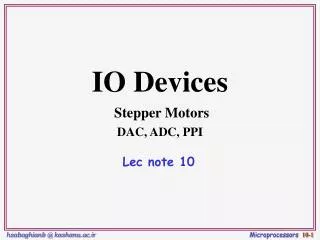
IO Devices Stepper Motors DAC, ADC, PPI. Lec note 10. Stepper Motors. more accurately controlled than a normal motor allowing fractional turns step by step low speed, and lower torque than a comparable D.C. motor useful for precise positioning for robotics

E N D
IO Devices Stepper MotorsDAC, ADC, PPI Lec note 10
Stepper Motors • more accurately controlled than a normal motor • allowing fractional turns step by step • low speed, and lower torque than a comparable D.C. motor • useful for precise positioning for robotics • Servomotors require a position feedback signal for control
Terminology • Steps per second(SPS), Rotate Per minute (RPM) • SPS = (RPM * SPR) /60 • Number of teeth • 4-step, wave drive 4-step, 8-step • Motor speed (SPS) • Holding torque
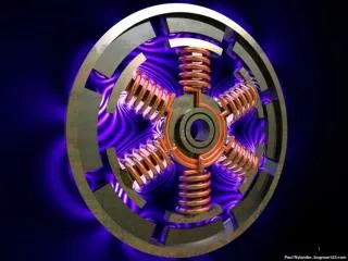
Stepper Motor Types • Variable Reluctance • Permanent Magnet
Variable Reluctance Motors • This is usually a four wire motor – the common wire goes to the +ve supply and the windings are stepped through • Our example is a 30o motor • The rotor has 4 poles and the stator has 6 poles • Example
Variable Reluctance Motors • To rotate we excite the 3 windings in sequence • W1 - 1001001001001001001001001 • W2 - 0100100100100100100100100 • W3 - 0010010010010010010010010 • This gives two full revolutions
Unipolar Motors • To rotate we excite the 2 windings in sequence • W1a - 1000100010001000100010001 • W1b - 0010001000100010001000100 • W2a - 0100010001000100010001000 • W2b - 0001000100010001000100010 • This gives two full revolutions
Unipolar Motors • To rotate we excite the 2 windings in sequence • W1a - 1100110011001100110011001 • W1b - 0011001100110011001100110 • W2a - 0110011001100110011001100 • W2b - 1001100110011001100110011 • This gives two full revolutions at 1.4 times greater torque but twice the power
Enhanced Waveforms • better torque • more precise control
Unipolar Motors • The two sequences are not the same, so by combining the two you can produce half stepping • W1a - 11000001110000011100000111 • W1b - 00011100000111000001110000 • W2a - 01110000011100000111000001 • W2b - 00000111000001110000011100
Motor Control Circuits • For low current options the ULN200x family of Darlington Arrays will drive the windings direct.
8255 • 8051 has limited number of I/O ports • one solution is to add parallel interface chip(s) • 8255 is a Programmable Peripheral Interface PPI • Add it to 8051 to expand number of parallel ports • 8051 I/O port does not have handshaking capability • 8255 can add handshaking capability to 8051
8255 • Programmable Peripheral Interface (PPI) • Has 3 8_bit ports A, B and C • Port C can be used as two 4 bit ports CL and Ch • Two address lines A0, A1 and a Chip select CS • 8255 can be configured by writing a control-word in CR register
8255 Operating Modes • Mode 0 : Simple I/O • Any of A, B, CL and CH can be programmed as input or output • Mode 1: I/O with Handshake • A and B can be used for I/O • C provides the handshake signals • Mode 2: Bi-directional with handshake • A is bi-directional with C providing handshake signals • B is simple I/O (mode-0) or handshake I/O (mode-1) • BSR (Bit Set Reset) Mode • Only C is available for bit mode access • Allows single bit manipulation for control applications
Mode 0 • Provides simple input and output operations for each of the three ports. • No “handshaking” is required, data is simply written to or read from a specified port. • Two 8-bit ports and two 4-bit ports. • Any port can be input or output. • Outputs are latched. • Inputs are not latched
Mode 1 • Mode 1 Basic functional Definitions: • Two Groups (Group A and Group B). • Each group has one 8-bit data port and one 4-bit control/data port. • The 8-bit data port can be either input or output. Both inputs and outputs are latched. • The 4-bit port is used for control and status of the 8-bit data port.
Mode 1 – Control Signals • Output Control Signal Definition • OBF (Output Buffer Full F/F). (C7 for A, C1 for B) • The OBF output will go “low” to indicate that the CPU has written data out to the specified port. • A signal to the device that there is data to be read. • ACK (Acknowledge Input). (C6 for A, C2 for B) • A “low” on this input informs the 8255 that the data from Port A or Port B has been accepted. • A response from the peripheral device indicating that it has read the data. • INTR (Interrupt Request). (C3 for A, C0 for B) • A “high” on this output can be used to interrupt the CPU when an output device has accepted data transmitted by the CPU.
Mode 1 – Control Signals • Input Control Signal Definition • STB (Strobe Input). (C4 for A, C2 for B) • A “low” on this input loads data into the input latch. • IBF (Input Buffer Full F/F) (C5 for A, C1 for B) • A “high” on this output indicates that the data has been loaded into the input latch; in essence, an acknowledgement from the 8255 to the device. • INTR (Interrupt Request) (C3 for A, C0 for B) • A “high” on this output can be used to interrupt the CPU when an input device is requesting service.
Mode 2 - Strobed Bidirectional Bus I/O • MODE 2 Basic Functional Definitions: • Used in Group A only. • One 8-bit, bi-directional bus port (Port A) and a 5-bit control port (Port C). • Both inputs and outputs are latched. • The 5-bit control port (Port C) is used for control and status for the 8-bit, bi-directional bus port (Port A).
Mode 2 • Output Operations • OBF (Output Buffer Full). The OBF output will go low to indicate that the CPU has written data out to port A. • ACK (Acknowledge). A low on this input enables the tri-state output buffer of Port A to send out the data. Otherwise, the output buffer will be in the high impedance state. • Input Operations • STB (Strobe Input). A low on this input loads data into the input latch. • IBF (Input Buffer Full F/F). A high on this output indicates that data has been loaded into the input latch.
BSR Mode • If used in BSR mode, then the bits of port C can be set or reset individually
BSR Mode example Move dptr, 0093h Up: Move a, 09h ;set pc4 Movx @dptr,a Acall delay Mov a,08h ;clr pc4 Movx @dptr,a Acall delay Sjmp up
Interfacing 8255 with 8051 • CS is used to interface 8255 with 8051 • If CS is generated from lets say Address lines A15:A12 as follows,A15:A13 = 110 • Address of 8255 is 110 xxxxx xxxx xx00b • Base address of 8255 is • 1100 0000 0000 0000b=C000H • Address of the registers • A = C000H • B = C001H • C = C002H • CR = C003H
Interfacing 8255 with 8051 P2.7(A15) P2.6(A14) P2.5(A13) A2 A1 A0 74138 3×8 decoder 8051 /CS 8255 A0 A1 ALE O0 O1 O7 74373 P0.7-P0.0 (AD7-AD0) D7-D0 D7-D0 /RD /WR /RD /WR