Kabuki 2800: Critical Design Review - Prototyping High-Performance Audio Processor System
480 likes | 561 Views
This project involves designing a high-performance audio processor system with components such as DSP co-processor, router board, FPGA, USB interface, and more. The system is aimed at delivering efficient signal processing and audio effects, with detailed specifications, software processes, test results, and a division of labor outlined. The design includes elements like A/D and D/A conversion, audio inputs and outputs, foot pedal actuators, and communication protocols. Development tasks are distributed among team members, with a focus on software effects, layout design, firmware development, and hardware fabrication. The project is scheduled into phases for development, integration, testing, and production.

Kabuki 2800: Critical Design Review - Prototyping High-Performance Audio Processor System
E N D
Presentation Transcript
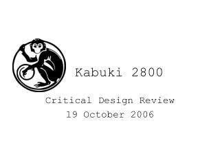
Kabuki 2800 Critical Design Review 19 October 2006
Agenda • System Block Diagram • Software Processes • System Specifications and Design • Test Results and Demo • Detailed Schedule • Division of Labor
DSP Co-Processor • FFT / IFFT • Communicates with DSK via HPI or Router Card • Audio Out • Analog • DSK Starter Kit • 48KHz A/D • 48KHz D/A • DSP processing core • Router Board • Routs signals between DSP host and all peripherals • FPGA and PROM • USB • RS-232 • USB display • Tablet or Laptop • Communicates with Router Card • Performance Board • A/D • Reads input from • 1 foot fader pedal • 5 actuators • Communicates with Router Card via RS-232 • Audio In • Analog Foot Pedal Actuator 1 Actuator 2 Actuator 3 Actuator 4 Actuator 5 Block Diagram Kabuki 2800
Router: Protocol • “Kabuki Router Advanced Addressing Protocol” • Common command and data protocol for all devices • 24-bit KRAAP packets • 3 bit dest. Module • 5 bit command code • 16 bits of data
Router: Logic example • USB asking UART command handler for input board state information
Software: DSP • Effects processing magic • Runs on TI DSK • Written entirely in C • Currently ~3k lines of code • Subversion version control
Software: DSP • Gets preset info from router • Gets inputs from input board or software console • Sends data to software console for spectral analysis • Sends data to possible DSP coprocessor
Software: DSP • Toplevel architecture
Software: DSP • Possible effect: Single
Software: DSP • Possible effect: Mixer
Software: DSP • Possible effect: Complex
Software: Console • Connects to router via USB • Written entirely in Python • Uses Gtk+ Linux GUI toolkit • ‘Subversion’ version control • Nanobunnies
Router Function: • Handles I/O from one module to the next • Brain: • FPGA with FLASH prom/memory • Ports: • EMIF, RS-232, USB, JTAG
Router Board EMIF DLP-245 Buttons MAX3237 74xx TXRX 3.3V USB RS-232 PROM HPI Cyclone II FPGA FLASH JTAG LEDs 1.2V CLK Buko the monkey PERIPH.
Max RS 3232 • Assembled • Prototyped • Capacitors • Lag time • Functionality
Prototype Board DB9 Connector RS3232
Performance Module Specifications • Read fader pedal from A/D @12 bits • Read foot actuator inputs • Boot from flash prom • Communicate with Router Board via RS-232 Transceiver at 1MHz • Debugging LEDs and Switches
RS-232 Transceiver Switches / LEDs Spartan 3E Flash PROM A/D Converter Foot Pedal Actuators Performance Block Diagram
Reset Performance Module Switches LEDs RS232 Transceiver VREG Vcc XilinxPROM A/D JTAG VREG VccAux Spartan3E FPGA Actuator Inputs Fader Pedal VREG VccInt
Performance Module Design • Xilinx Spartan 3E FPGA to handle communication with the A/D and Router Card. • Xilinx PROM to program Spartan 3E • Maxim 3237 RS-232 Megabaud Transceiver Clock Source: Crystal Oscillator (25-100MHz)
Performance Module Input • 5 Foot Actuators • (Connected directly into Spartan) • 1 Fader Foot Pedal • 3.3 volt signal attenuated through the pedal • AD7859 (ADC with 12-bit resolution) • High speed • PLCC 44 package: replaceable • 8 LEDs, 8 Switches, 1 Reset Button
Performance Module Power • Vcc = 3.3 V LDO Regulator LT1086, stepped down from 5 V • JTAG, VccAux = 2.5 V LDO Regulator LT1763, stepped down from 3.3 V Regulator • VccInt = 1.2 V LDO Regulator LT3021, stepped down from 3.3 V Regulator
DSP Co-processor Design TMS3206713B-200 • 200pin HLQFP • Not BGA!!! • Connection • through Host Peripheral Interface on DSK • 192K internal SRAM • Maybe enough! • Clock Source: • same as DSK, 50MHz Crystal Oscillator. HPI
DSP C -processor Specifications • Communication via 225MHz • Direct Connection to DSK Host • Transfer 256 samples and FFT / IFFT in <1us
Development Structure Primary Secondary Kabuki 2800
Dan’s Tasks Primary • Software Effects • Software Devices • Software simulation Secondary • Layout design and fabrication. • Firmware Kabuki 2800
Justin’s Tasks Primary • Router Board Layout Design and Fab. • Firmware • USB design and Protocols Secondary • Does No have any. Kabuki 2800
Tim’s Tasks Primary • Performance board firmware • layout and design Secondary • USB Design and Protocols • Device Casing Kabuki 2800
Yazan Task’s Primary • Device Casing and Fabrication • DSK and interface Card Secondary • Module hardware design • Module Firmware design • Audio effect algorithm simulation • Audio effect algorithm • Final packaging and Software Kabuki 2800
Schedule • Phase 1 – Milestone 1, Nov. 2 • Phase 2 – Milestone 2, Nov. 30 • Phase 3 – Expo, Dec. 14
Phases • Phase 1 – Development & Prototyping • Phase 2 – Integration • Phase 3 – Testing and Production
Router BoardPhase 1 • Board Fabricated (Done) • FPGA configured (Done) • FPGA boots from PROM (Done) • FLASH reads/writes properly • DSK I/O Firmware Complete • USB tested • RS-232 interface tested
Router BoardPhase 2 • FPGA configured and tested
Router BoardPhase 3 • All interfaces fully functional (RS-232, USB) • Flash storage able to load / store presets • I/O functions with DSK and DSP co-processor • USB firmware interfaces with FPGA and with host computer • RS-232 interface fully functioning • Firmware completed and under testing • Communication established with DSP coprocessor.
Performance BoardPhase 1 • PCB Fabricated (In Progress) • FPGA configured and tested • FPGA boots from EEPROM • A/D converter tested • Firmware in testing
Performance BoardPhase 2 • FPGA interfaces with I/O board • Foot – pedals generate interrupts • A/D converter samples fader pedal
Performance BoardPhase 3 • FPGA interfaces with Interface Card • All user inputs are fully functional
DSP Coprocessor Phase 1 • Board Layout Complete
DSP Coprocessor Phase 2 • Board fabricated, populated and ready for testing • JTAG ready
DSP Coprocessor Phase 3 • DSP Processor is able to implement FFT and Wavelet Transforms • DSP is able to communicate with I/O board and and co-process transforms
Effect Algorithms Phase 1 • Some Time Domain Effects Simulated • Phasing • Filters • Etc.
Effect Algorithms Phase 2 • Most time domain effects simulated • Several more time domain effects implemented • FFTs simulated in Matlab
Effect Algorithms Phase 3 • Time Domain effects implemented • FFT and Wavelet Domain effects simulated and implemented