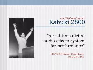
Kabuki 2800
480 likes | 664 Views
Kabuki 2800. Critical Design Review 19 October 2006. Agenda. System Block Diagram Software Processes System Specifications and Design Test Results and Demo Detailed Schedule Division of Labor. DSP Co-Processor FFT / IFFT Communicates with DSK via HPI or Router Card. Audio Out Analog.

Kabuki 2800
E N D
Presentation Transcript
Kabuki 2800 Critical Design Review 19 October 2006
Agenda • System Block Diagram • Software Processes • System Specifications and Design • Test Results and Demo • Detailed Schedule • Division of Labor
DSP Co-Processor • FFT / IFFT • Communicates with DSK via HPI or Router Card • Audio Out • Analog • DSK Starter Kit • 48KHz A/D • 48KHz D/A • DSP processing core • Router Board • Routs signals between DSP host and all peripherals • FPGA and PROM • USB • RS-232 • USB display • Tablet or Laptop • Communicates with Router Card • Performance Board • A/D • Reads input from • 1 foot fader pedal • 5 actuators • Communicates with Router Card via RS-232 • Audio In • Analog Foot Pedal Actuator 1 Actuator 2 Actuator 3 Actuator 4 Actuator 5 Block Diagram Kabuki 2800
Router: Protocol • “Kabuki Router Advanced Addressing Protocol” • Common command and data protocol for all devices • 24-bit KRAAP packets • 3 bit dest. Module • 5 bit command code • 16 bits of data
Router: Logic example • USB asking UART command handler for input board state information
Software: DSP • Effects processing magic • Runs on TI DSK • Written entirely in C • Currently ~3k lines of code • Subversion version control
Software: DSP • Gets preset info from router • Gets inputs from input board or software console • Sends data to software console for spectral analysis • Sends data to possible DSP coprocessor
Software: DSP • Toplevel architecture
Software: DSP • Possible effect: Single
Software: DSP • Possible effect: Mixer
Software: DSP • Possible effect: Complex
Software: Console • Connects to router via USB • Written entirely in Python • Uses Gtk+ Linux GUI toolkit • ‘Subversion’ version control • Nanobunnies
Router Function: • Handles I/O from one module to the next • Brain: • FPGA with FLASH prom/memory • Ports: • EMIF, RS-232, USB, JTAG
Router Board EMIF DLP-245 Buttons MAX3237 74xx TXRX 3.3V USB RS-232 PROM HPI Cyclone II FPGA FLASH JTAG LEDs 1.2V CLK Buko the monkey PERIPH.
Max RS 3232 • Assembled • Prototyped • Capacitors • Lag time • Functionality
Prototype Board DB9 Connector RS3232
Performance Module Specifications • Read fader pedal from A/D @12 bits • Read foot actuator inputs • Boot from flash prom • Communicate with Router Board via RS-232 Transceiver at 1MHz • Debugging LEDs and Switches
RS-232 Transceiver Switches / LEDs Spartan 3E Flash PROM A/D Converter Foot Pedal Actuators Performance Block Diagram
Reset Performance Module Switches LEDs RS232 Transceiver VREG Vcc XilinxPROM A/D JTAG VREG VccAux Spartan3E FPGA Actuator Inputs Fader Pedal VREG VccInt
Performance Module Design • Xilinx Spartan 3E FPGA to handle communication with the A/D and Router Card. • Xilinx PROM to program Spartan 3E • Maxim 3237 RS-232 Megabaud Transceiver Clock Source: Crystal Oscillator (25-100MHz)
Performance Module Input • 5 Foot Actuators • (Connected directly into Spartan) • 1 Fader Foot Pedal • 3.3 volt signal attenuated through the pedal • AD7859 (ADC with 12-bit resolution) • High speed • PLCC 44 package: replaceable • 8 LEDs, 8 Switches, 1 Reset Button
Performance Module Power • Vcc = 3.3 V LDO Regulator LT1086, stepped down from 5 V • JTAG, VccAux = 2.5 V LDO Regulator LT1763, stepped down from 3.3 V Regulator • VccInt = 1.2 V LDO Regulator LT3021, stepped down from 3.3 V Regulator
DSP Co-processor Design TMS3206713B-200 • 200pin HLQFP • Not BGA!!! • Connection • through Host Peripheral Interface on DSK • 192K internal SRAM • Maybe enough! • Clock Source: • same as DSK, 50MHz Crystal Oscillator. HPI
DSP C -processor Specifications • Communication via 225MHz • Direct Connection to DSK Host • Transfer 256 samples and FFT / IFFT in <1us
Development Structure Primary Secondary Kabuki 2800
Dan’s Tasks Primary • Software Effects • Software Devices • Software simulation Secondary • Layout design and fabrication. • Firmware Kabuki 2800
Justin’s Tasks Primary • Router Board Layout Design and Fab. • Firmware • USB design and Protocols Secondary • Does No have any. Kabuki 2800
Tim’s Tasks Primary • Performance board firmware • layout and design Secondary • USB Design and Protocols • Device Casing Kabuki 2800
Yazan Task’s Primary • Device Casing and Fabrication • DSK and interface Card Secondary • Module hardware design • Module Firmware design • Audio effect algorithm simulation • Audio effect algorithm • Final packaging and Software Kabuki 2800
Schedule • Phase 1 – Milestone 1, Nov. 2 • Phase 2 – Milestone 2, Nov. 30 • Phase 3 – Expo, Dec. 14
Phases • Phase 1 – Development & Prototyping • Phase 2 – Integration • Phase 3 – Testing and Production
Router BoardPhase 1 • Board Fabricated (Done) • FPGA configured (Done) • FPGA boots from PROM (Done) • FLASH reads/writes properly • DSK I/O Firmware Complete • USB tested • RS-232 interface tested
Router BoardPhase 2 • FPGA configured and tested
Router BoardPhase 3 • All interfaces fully functional (RS-232, USB) • Flash storage able to load / store presets • I/O functions with DSK and DSP co-processor • USB firmware interfaces with FPGA and with host computer • RS-232 interface fully functioning • Firmware completed and under testing • Communication established with DSP coprocessor.
Performance BoardPhase 1 • PCB Fabricated (In Progress) • FPGA configured and tested • FPGA boots from EEPROM • A/D converter tested • Firmware in testing
Performance BoardPhase 2 • FPGA interfaces with I/O board • Foot – pedals generate interrupts • A/D converter samples fader pedal
Performance BoardPhase 3 • FPGA interfaces with Interface Card • All user inputs are fully functional
DSP Coprocessor Phase 1 • Board Layout Complete
DSP Coprocessor Phase 2 • Board fabricated, populated and ready for testing • JTAG ready
DSP Coprocessor Phase 3 • DSP Processor is able to implement FFT and Wavelet Transforms • DSP is able to communicate with I/O board and and co-process transforms
Effect Algorithms Phase 1 • Some Time Domain Effects Simulated • Phasing • Filters • Etc.
Effect Algorithms Phase 2 • Most time domain effects simulated • Several more time domain effects implemented • FFTs simulated in Matlab
Effect Algorithms Phase 3 • Time Domain effects implemented • FFT and Wavelet Domain effects simulated and implemented