Download
1 / 41
420 likes | 567 Views
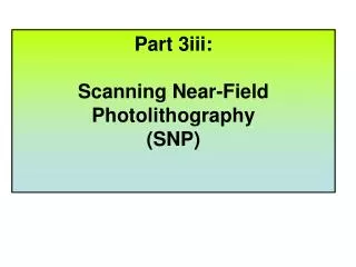
Part 3iii: Scanning Near-Field Photolithography (SNP). Learning Objectives. After completing PART 3iii of this course you should have an understanding of, and be able to demonstrate, the following terms, ideas and methods. The photo-oxidation process of thiolates to sulfonates on gold,

E N D
Part 3iii: Scanning Near-Field Photolithography (SNP)
Learning Objectives • After completing PART 3iii of this course you should have an understanding of, and be able to demonstrate, the following terms, ideas and methods. • The photo-oxidation process of thiolates to sulfonates on gold, • Appreciate how the surface chemistry is probed by various spectroscopic techniques, • Appreciate how the modified surfaces can be utilised as platforms for building the structures into the third dimension, • Appreciate the various chemistries that are initiated by the radiation, • Appreciate how an AFM operates, • Appreciate how a SNOM operates, and • Appreciate how SNP works
Background Some Surface Photo-oxidation Chemistry
S H S O 3 Photoxidation of Thiol SAMs on Golds and Silver XPS Immersion for 1 Hr in 1 mM Hexane thiol solution I Hr UV irradiation in air J. Am. Chem. Soc.1993, 115, 5305
Static SIMS 10 Mins Photooxidation 40 Mins Photooxidation J. Am. Chem. Soc. 2001, 123, 4089-4090
Mask Patterning the C60 Film SIMS 254 nm Photooxidation
Background An Atomic Force Microscope (AFM)
A key element of the AFM is its force sensor, or cantilever. The cantilever is usually formed by one or more beams of silicon or silicon nitride that is 100 to 500 microns long and about 0.5 to 5 microns thick. Mounted on the end of the cantilever is a sharp tip that is used to sense a force between the sample and tip. For normal topographic imaging, the probe tip is brought into continuous or intermittent contact with the sample and scanned over the surface. Fine-motion piezoelectric scanners generate the precision motion needed to generate topographic images and force measurements. A piezoelectric scanner is a device that moves by a sub-nanomtere amountswhen a voltage is applied across its electrodes. Depending on the AFM design, scanners are used to translate either the sample under the cantilever or the cantilever over the sample. Piezoelectric scanners for AFMs usually can translate in three directions (x, y, and z axes) and come in different sizes to allow maximum scan ranges of 0.5 to 125 microns in the x and y axes and several microns in the vertical (z) axis. A well-built scanner can generate stable motion on a scale below 1 Angstrom. By scanning the AFM cantilever over a sample surface (or scanning a sample under the cantilever) and recording the deflection of the cantilever, the local height of the sample is measured. Three-dimensional topographical maps of the surface are then constructed by plotting the local sample height versus horizontal probe tip position
The AFM Cantilever and Tip The Tip is an Atom!! Tip Atomic Resolution
Background Scanning Near Field Optical Microscope (SNOM)
SNOM/NSOM http://www.olympusmicro.com/primer/techniques/nearfield/nearfieldhome.html Drawn or etched fibre optic cable appended to AFM cantilever Or hole made in the end of an AFM tip Wavelength of light 180-300 nm i.e. longer than the aperture l Therefore diffraction… Which is limited by being used in the near field Aperture ~50 nm ~10 nm
SNOM/NSOM http://www.olympusmicro.com/primer/techniques/nearfield/nearfieldintro.html Strands of DNA http://www.witec.de/pdf/alpha300Sflyer.pdf
The SNOM as Lithography Tool Scanning Near Field Photolithograpgy
Au Scanning Near Field Photolithography, Oxidation and Back Filling 6 6 6 S N O M J. Am. Chem. Soc., 2002,124, 2414
AFM (Friction Force Mode) CH3 CO2H Lines 6 x 6 mm J. Am. Chem. Soc., 2002,124, 2414
Au Scanning Near Field Photolithography, Oxidation and Etching Fe(CN)62+/Fe(CN)63+ (aq) 30 mins 11 11 S N O M S H S O 3
Chemical Modifying the SAM Surface Group NANO LETTERS, 2006, 6, 29-33 hm hm DNA [O]
(i) Convert acid into active ester (ii) Incubate with Calf Thymus DNA
S O O S 3 3 S O S O 3 3 S O 3 UV Radiation S O S O S O 3 3 3 S O S O 3 3 Aggregation of Gold Writing to Gold Nanoparticles on SiO2 Nanoletters, 2006, 6, 345
Decane thiol passivated gold nanoparticles (1-3 nm) M. Brust, M. Walker, D. Bethell, D. J. Schiffrin, R. Whyman, J. Chem. Soc., Chem. Commun.,1994, 801-802. Si/SiO2 Spinning Making a Thin Film of Nanoparticles: Spin Coating Volatile solvent Solvent evaporates
10mm Parallel Exposure to 244 nm photons Irradiation/Rinsing UV Masks 2nm 40nm Si/SiO2 Si/SiO2 Si/SiO2 70 nm Rinse Unirradiated particles rinse away Making 3D Micron Scale Structures
100 nm 10 nm 2 nm 40 nm Si/SiO2 Si/SiO2 Si/SiO2 x Rinse z y Proposal: Scanning Near Field Photolithography (SNP)
100 nm 10 nm 2 nm 40 nm Si/SiO2 Si/SiO2 Si/SiO2 250 nm 120 nm 110 nm x Rinse 14 nm z y Proposal: Scanning Near Field Photolithography (SNP) This was a little disappointing as structures were greater than 100 nm
Solution? Making a Thinner Film of the Gold Nanoparticles Langmuir-Schaeffer Layer Structures Repeat to obtain a bilayer Air Moveable Barrier Water
Langmuir-Schaeffer Bilayers and SNP Structures 60 nm 60 nm structures indicates that the excitation does not spread outside the area illuminated by the probe, in contrast to the behavior observed for the spin-cast films. ~ SNOM Aperture 6 nm High ~2 x diameter of the particles The structures are continuous and appear generally free from defects, with some thinning.
1mm e e - + Writing Wires Making Carbon Nanowires with Photons: Scanning Near Field Photolithography Parvez Iqbal†, Marcus D Hanswell‡, Shuqing Sun,# Tim Richardson‡, G. Leggett# and Jon A. Preece† †School of Chemistry, University of Birmingham, Edgbaston, Birmingham B15 2TT ‡ Department of Physics and Astronomy, University of Sheffield, S3 7RH School of Chemistry, University of Sheffield,Western Bank, Sheffield, S10 2TN
~ 1 nm Reaction of C60 Under UV Light Exposure • Rao et al. demonstrated UV light exposure on C60 film led to a insoluble material in toluene • Through Raman and infrared spectroscopy, x-ray diffraction and Laser desorption mass spectroscopy concluded that the exposed C60 film underwent photopolymerisation (2 + 2 cycloaddition) For Yr2 and Yr3 Chemists!! p2s + p2s Photochemical Cycloaddition LUMO (ene) SOMO (ene) Combination UV light M. Rao, P. Zhou, K.-A. Wang, G. T. Hagar, J. M. Holden, Y. Wang, W.-T. Lee, X.-X. Bi, P. C. Eklund, D. S. Cornett, . M. A. Duncan, I. J. Amster, Science, 1993, 259, 955
5 mm min-1 Making a Thin Film of C60 Langmuir-Blodgett Layer Structures Air ~ 2.5 nm Moveable Barrier Water
Mask Patterning the C60 Film Substrate
Patterning the C60 Film with SNP 0.3 mm s-1 1 mm s-1 2 mm s-1 35 mm s-1
Conclusions on SNP SNP is a very facile and versatile route to create nanostructured surfaces, with resolution better than photolithography and almost equalling EBL. It requires relatively cheap instrumentation and is carried out under ambient conditions. Only the tip of the iceberg has been looked at to date as to what type of SAMs and functional groups might be modified, and there is a whole host of chemical reactions that have been studied in the solution phase that could be transferred to the surface. Major disadvantage of SNP (and EBL) is that it is a serial process and therefore slow, unlike photolithography.
Summing Up Part 3 Photolithography is a rapid parallel process, but is struggling with to keep pace with Moore’s law. E-beam lithography is a slow serial process, but can create nanoscale structures. However, it requires the use of expensive intrumentation and UHV conditions. SNP is a slow serial process, but can also create nanoscale structures. In addition, it is a relative cheap and facile methodology, being carried out under ambient conditions.
MAPPER An array of around 14,000 direct write electron beams
Millipede An Array of AFM cantilvers and tips http://www.zurich.ibm.com/st/storage/concept.html#