MIPS תיאור מפושט של מעבד
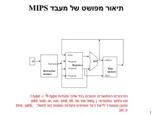
MIPS תיאור מפושט של מעבד. החיבורים המתוארים תומכים בכל שלבי פקודות R-type ו- I-type אנו נתמוך בפקודות: add, sub, or, xor, and, slt, lw, sw, beq, j כמובן שנצטרך לדעת כיצד מוסיפים פקודות נוספות כמו למשל: bne, addi, jal, jr. עוד שלושה שבועות. שלבי ביצוע הוראת מכונה.

MIPS תיאור מפושט של מעבד
E N D
Presentation Transcript
MIPS תיאור מפושט של מעבד החיבורים המתוארים תומכים בכל שלבי פקודות R-typeו- I-type אנו נתמוך בפקודות: add, sub, or, xor, and, slt, lw, sw, beq, j כמובן שנצטרך לדעת כיצד מוסיפים פקודות נוספות כמו למשל: bne, addi, jal, jr
שלבי ביצוע הוראת מכונה (1) FETCH = קרא הוראה מהזיכרון ע"פ הכתובת שמכיל ה-PC. (2) DECODE = פענח את הפקודה וקרא את האוגרים הנחוצים (אחד או שניים). (3) EXECUTE = בעזרת ה-ALUחשב את התוצאה, או כתובת רצויה. (4) MEMORY = השתמש בתוצאה לבצע במידת הצורך: או טעינה לזיכרון (Store) או קריאה מהזיכרון (Load). (5) WRITE BACK = בצע במידת הצורך טעינה לאוגר.
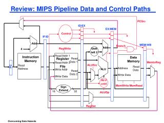
במשך כל מחזור השעון קוראים בסוף השעון כותבים falling edge cycle time rising edge קווי הבקרה - מיוצרים על פי השעון, כל עליית שעון תשנה בעקבותיה את קווי הבקרה (אם נדרש)
Single cycle data paths D Q All state elements act like positive edge-triggered flip flops. clk Processor uses synchronous logic design (a “clock”).
Edge-Triggered D Flip Flops D Q CLK Value of D is sampled on positive clock edge. Q outputssampledvalue for rest of cycle. D Q
Single cycle data paths: Definition All instructions execute in a singlecycle of the clock (positive edge to positive edge) Advantage: a great way to learn CPUs. Drawbacks: unrealistic hardware assumptions, slow clock period
Recall: MIPS R-format instructions Instruction Fetch opcode rs rt rd shamt funct Instruction Decode Decode fields to get : ADD $8 $9 $10 Operand Fetch Execute Result Store Next Instruction Syntax: ADD $8 $9 $10 Semantics: $8 = $9 + $10 Fetch next inst from memory:012A4020 “Retrieve” register values: $9 $10 Add $9 to $10 Place this sum in $8 Prepare to fetch instruction that follows the ADD in the program.
Separate Read-Only Instruction Memory זכרון פקודות 32 Data Addr 32 Reads are combinational: Put a stable address on input, a short time later data appears on output. זכרון (מטמון) נפרד לפקודות ולנתונים (Instruction Memory & Data Memory) טעינת התוכנית לזכרון לא מעניננו כרגע
שלב 1: Straight-line Instruction Fetch Instr Mem 32 Data Addr 32 CLK Addr PC PC + 4 PC + 8 IMem[PC + 4] Data IMem[PC] IMem[PC + 8] PC == Program Counter, points to next instruction. Fetching straight-line MIPS instructions requires a machine that generates this timing diagram: Why do we increment every clock cycle? Why +4 and not +1?
Single-cycle Implementation of MIPS • Our first implementation of MIPS will use a single long clock cycle for every instruction • Every instruction begins on one up (or, down) clock edge and ends on the next up (or, down) clock edge • This approach is not practical as it is much slower than a multicycle implementation where different instruction classes can take different numbers of cycles • in a single-cycle implementation every instruction must take the same amount of time as the slowest instruction • in a multicycle implementation this problem is avoided by allowing quicker instructions to use fewer cycles • Even though the single-cycle approach is not practical it is simple and useful to understand first • Note : we shall implement jump at the very end
New Component: Register (for PC) Built out of an array of 32 flip-flops Din0 D Q Dout0 D Q Din1 Dout1 Din2 Dout2 D Q clk PC 32 32 Din Dout Clk In later examples, we will add an “enable” input: clock edge updates state only if enable is high
New Component: A 32-bit adder (ALU) 32 Combinational: היציאה שווה לסכום ערכי כניסה A ו-B מלפני זמן קצר (~ ננו שניה). A 32 A + B + 32 B op ALU: כנ"ל רק למס פונקציות רבות לפי הבורר op. 32 ln(#ops) A 32 ALU A op B 32 Zero? B Sometimes, extra outputs for use by control logic ...
Design: Straight-line Instruction Fetch CLK Addr PC PC + 4 PC + 8 IMem[PC + 4] Data IMem[PC] IMem[PC + 8] State machine design in the service of an ISA Instr Mem 32 PC 32 32 32 Addr Data D Q + 32 32 0x4 +4 in hexadecimal Clk
Goal #1: An R-format single-cycle CPU Done! To continue, we need registers ... Instruction Fetch opcode rs rt rd shamt funct Instruction Decode Decode fields to get : ADD $8 $9 $10 Operand Fetch Execute Result Store Next Instruction Syntax: ADD $8 $9 $10 Semantics: $8 = $9 + $10 Fetch next inst from memory:012A4020 “Retrieve” register values: $9 $10 Add $9 to $10 Place this sum in $8 Prepare to fetch instruction that follows the ADD in the program.
Register files: clk “two read ports” sel(rs1) sel(ws) 5 5 R0 - The constant 0 Q 32 32 ... MUX rd1 DEMUX ... . . WE 32 ... sel(rs2) 5 32 32 MUX ... rd2 32 wd Why is R0 special? En Q R1 D En Q R2 D ... En R31 Q D 32
Register File Schematic Symbol RegFile 5 rs1 32 5 rd1 rs2 5 ws 32 rd2 wd WE 32 Why do we need WE (Write Enable)? If we had a register file w/o WE, how could we work around it?
Datapath: Instruction Store/Fetch & PC Increment Three elements used to store and fetch instructions and increment the PC Datapath
Animating the Datapath Instruction <- MEM[PC] PC <- PC + 4
Datapath: R-Type Instruction Two elements used to implement R-type instructions Datapath
Animating the Datapath add rd, rs, rt R[rd] <- R[rs] + R[rt];
Datapath: Load/Store Instruction Two additional elements used To implement load/stores Datapath
Animating the Datapath lw rt, offset(rs) R[rt] <- MEM[R[rs] + s_extend(offset)];
Animating the Datapath sw rt, offset(rs) MEM[R[rs] + sign_extend(offset)] <- R[rt]
Datapath: Branch Instruction No shift hardware required: simply connect wires from input to output, each shifted left 2 bits Datapath
Animating the Datapath beq rs, rt, offset • if (R[rs] == R[rt]) then PC <- PC+4 + s_extend(offset<<2)
MIPS Datapath I: Single-Cycle Input is either register (R-type) or sign-extended lower half of instruction (load/store) Data is either from ALU (R-type) or memory (load) Combining the datapaths for R-type instructions and load/stores using two multiplexors
Animating the Datapath: R-type Instruction add rd,rs,rt
Animating the Datapath: Load Instruction lw rt,offset(rs)
Animating the Datapath: Store Instruction sw rt,offset(rs)
MIPS Datapath II: Single-Cycle Separate adder as ALU operations and PC increment occur in the same clock cycle Separate instruction memory as instruction and data read occur in the same clock cycle Adding instruction fetch
MIPS Datapath III: Single-Cycle New multiplexor Extra adder needed as both adders operate in each cycle Instruction address is either PC+4 or branch target address Adding branch capability and another multiplexor Important note: in a single-cycle implementation data cannot be stored during an instruction – it only moves through combinational logic Question: is the MemRead signal really needed?! Think of RegWrite…!
Datapath Executing add add rd, rs, rt
Datapath Executing lw lw rt,offset(rs)
Datapath Executing sw sw rt,offset(rs)
Datapath Executing beq beq r1,r2,offset
Goal #1: An R-format single-cycle CPU What do we do with these? Instruction Fetch opcode rs rt rd shamt funct Instruction Decode Decode fields to get : ADD $8 $9 $10 Operand Fetch Execute Result Store Next Instruction Syntax: ADD $8 $9 $10 Semantics: $8 = $9 + $10 Fetch next inst from memory:012A4020 “Retrieve” register values: $9 $10 Add $9 to $10 Place this sum in $8 Prepare to fetch instruction that follows the ADD in the program.
Computing engine of the R-format CPU opcode rs rt rd shamt funct op 32 RegFile 5 rs1 32 5 rd1 32 ALU rs2 5 ws 32 rd2 32 wd WE 32 Decode fields to get : ADD $8 $9 $10 Logic What do we do with WE?
Putting it all together ... Instr Mem 32 PC 32 32 32 Addr Data D Q + 32 32 0x4 op 32 RegFile 5 rs1 32 5 rd1 32 ALU rs2 5 ws 32 rd2 32 wd WE 32 To rs1, rs2, ws, op decode logic ... Logic Is it safe to use same clock for PC and RegFile?
Reminder: How data flows after posedge Instr Mem Addr Data + 0x4 Logic op 32 RegFile 5 rs1 32 5 rd1 32 ALU rs2 5 ws 32 rd2 32 wd WE 32 PC D Q
Next posedge: Update state and repeat RegFile 5 rs1 32 5 rd1 rs2 5 ws 32 rd2 wd WE 32 PC D Q
A CPU capable of R-type instructions only [25:21]=Rs [20:16]=Rt [15:11]=Rd 5 5 5 ck איך זה נראה בספר? 4 Adder [31:26] 6 Instruction Memory PC [5:0]=funct 6
A CPU capable of R-type instructions only [25:21]=Rs [20:16]=Rt [15:11]=Rd 5 5 5 ck ck איך זה נראה בספר? 4 Adder [31:26] 6 Reg File Instruction Memory PC ALU [5:0]=funct 6
A CPU capable of R-type instructions only [25:21]=Rs [20:16]=Rt [15:11]=Rd 5 5 5 ck ck איך זה נראה בספר? 4 Adder [31:26] 6 Reg File Instruction Memory PC ALU [5:0]=funct 6
יעד מס 2: I-format ALU instructions In this example, $8 (the result register) is rt !!! (was rd previously). 16-bit immediate extended to 32 bits. Syntax: ORI $8 $9 64 Semantics: $8 = $9 | 64 Zero-extend: 0x8000 ⇨ 0x00008000 Sign-extend: 0x8000 ⇨ 0xFFFF8000 Some MIPS instructions zero-extend immediate field, other instructions sign-extend.
Computing engine of the I-format CPU Logic op 32 RegFile 5 rs1 32 32 ALU 5 rd1 rs2 5 32 ws 32 rd2 Ext wd WE 32 Decode fields to get : ORI $8 $9 64 32 32 In a Verilog implementation, what should we do with rs2?
“two read ports” Merging data paths ... Add muxes R-format How many ? I-format Where ?
The merged data path ... opcode rs rt rd shamt funct op 32 RegFile 5 rs1 32 5 rd1 32 ALU rs2 5 ws 32 rd2 32 wd RegDest WE 32 Ext ALUsrc ExtOp ALUctr
Loads, Stores, and Data Memory ... Reads are combinational: Put a stable address on Addr, a short time later Doutis ready Data Memory 32 Addr 32 Dout Din 32 WE Syntax: LW $1, 32($2) Syntax: SW $3, 12($4) Action: $1 = M[$2 + 32] Action: M[$4 + 12] = $3 Zero-extend or sign-extend immediate field? Writes are clocked: If WE is high, memory Addr captures Dinon positive edge of clock. Note: Not a realistic main memory (DRAM) model ...
איפה ה- CPU? Instruction Memory CPU PC Data Memory