Download
1 / 14
150 likes | 861 Views
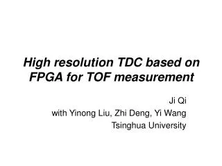
The 10-ps TDC implemented in an FPGA. Jinhong Wang, Shubin Liu, and Qi An FELab@USTC. Outline. Implementation of FPGA TDC @ USTC Timing Performance of FPGA TDC TDC Modules @ USTC. The Principle of the FPGA TDC. Coarse Counter ( Coarse Time ) + Time Interpolation within

E N D
The 10-ps TDC implemented in an FPGA Jinhong Wang, Shubin Liu, and Qi An FELab@USTC
Outline • Implementation of FPGA TDC @ USTC • Timing Performance of FPGA TDC • TDC Modules @ USTC
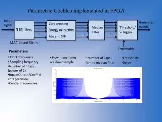
The Principle of the FPGA TDC • Coarse Counter (Coarse Time)+Time Interpolation within • one clock period (Fine Time)
Implementation of the Time Interpolation • Time Interpolation with the delay of Carry lines a) Carry-in in a Slice c) Carry chain of a multibit adder b) Rout in a SLICE
FPGA TDC @FELab, USTC • ~100 ps Bin Size, 50 ps RMS ; In the year 2005 TNS Vol.53, Issue 1 Part 2 Time interpolation with the dedicated Carry lines • ~50 ps Bin Size, < 20 ps RMS ; In the year 2009 TNS Vol.57, Issue 2 Part 1 With Several Compensation Strategies: self-test, Temperature compensation • Up to the present ~ 10 ps Bin Size (Effective) , <10 ps RMS a Modified Wave Union TDC
The 10-ps FPGA TDC Wave Union Launcher INV+Delay+MUX
Signal Processing of the Raw TDC Time N times Oscillation
Timing Performance • Uneven of the tap delay + Uncertainty of the Osc. Period • σosc << σcell • σosc ≈ σcell • σosc >> σcell 3 Simulation 2 1 Actual implementation falls in to Case 2 RMS vs. N
Timing Performance • Bin Size scales as 1/N Similar to dither Bin VS. N
FPGA TDC Module • ~20 ps RMS, 50 ps Bin NIM, USB, other platforms Xilinx, Altera • < 10 ps RMS, 12 ps Bin (planed) PXI, VME, USB Xilinx Virtex 4, Virtex 5…
The 25-ps FPGA TDC Module Altera + XILINX <25 ps RMS, 50 ps Bin
The 10-ps FPGA TDC Module • 16 + Chnl. • <10 ps RMS , ~10 ps Bin • Virtex 4 / Virtex 5, … • Platform: VME, PXI, USB 2.0 • Others: Trigger Matching