Download
1 / 16
160 likes | 392 Views
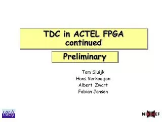
TDC in ACTEL FPGA. Tom Sluijk Wilco Vink Albert Zwart Fabian Jansen. 2 x ASDBLR. 2 x ASDBLR. 2 x ASDBLR. 2 x ASDBLR. LVDS Drivers. LVDS Drivers. LVDS Drivers. LVDS Drivers. FPGATDC 16ch. FPGATDC 16ch. FPGATDC 16ch. FPGATDC 16ch. Replaces OtisBoard. Replaces OtisBoard.

E N D
TDC in ACTEL FPGA Tom Sluijk Wilco Vink Albert Zwart Fabian Jansen
2 x ASDBLR 2 x ASDBLR 2 x ASDBLR 2 x ASDBLR LVDS Drivers LVDS Drivers LVDS Drivers LVDS Drivers FPGATDC 16ch FPGATDC 16ch FPGATDC 16ch FPGATDC 16ch Replaces OtisBoard Replaces OtisBoard Replaces OtisBoard Replaces OtisBoard OT FE Upgrate proposal (40 MHz) FPGATDC 16ch FPGATDC 16ch FPGATDC 16ch FPGATDC 16ch 2 x GBTX 10 Gb/s 2 x GBTX 10 Gb/s 2 x GBTX 10 Gb/s 2 x GBTX 10 Gb/s Replaces Gol/Aux Board 8 Fibers 40 Gb/s Outer Tracker Upgrade
TDC in Actel FPGA • Design of TDC in ACTEL Proasic3E FPGA because of the radiation properties • 16 Channel 4 bit TDC (bin size 1570 ps) • Zero Suppress or Raw data formats • Output 20 bit LVDS @ 160 MHz to GBT • I2C interface to set Mask Register, data format and read Histogrammer Outer Tracker Upgrade
Compile Report Family : ProASIC3E Device : A3PE1500 Package : 208 PQFP CORE Used: 13780 Total: 38400 (35.89%) IO (W/ clocks) Used: 89 Total: 147 (60.54%) Differential IO Used: 26 Total: 65 (40.00%) GLOBAL (Chip+Quadrant) Used: 8 Total: 18 (44.44%) PLL Used: 1 Total: 2 (50.00%) RAM/FIFO Used: 50 Total: 60 (83.33%) Low Static ICC Used: 0 Total: 1 (0.00%) FlashROM Used: 0 Total: 1 (0.00%) User JTAG Used: 0 Total: 1 (0.00%) Outer Tracker Upgrade
TDC (1 Channel) • PLL generates 3 clock signals; 8x Bx (320 MHz), 4x Bx (160MHz), 2x Bx (80 MHz) • 2 Phase Shifters, one shifts on the positive edge and the other on the negative edge of the 320 MHz clock, dividing the Bx in 16 phases • The Hit signal latches the state of the Phase shifters in the Hit Register • The LUT translates the 8 bit Hit Register into 4 bit time info • The Hit Logic decides if a valid hit occurred Outer Tracker Upgrade
Timing Diagram • Hits in the first half period of Bx (yellow bar) are tested in the second half period • Hits in the second half period are tested in the first half of Bx+1 • This causes a dead time of less then a Bx, only if a valid hit was detected • The Output Register is clocked in the middle of Bx+1 Outer Tracker Upgrade
FIFO Writer • Adds Bx Counter to the TDC data • Zero Suppresses the data • Possibility to bypass the Zero Suppressor Outer Tracker Upgrade
Zero Suppress • 4 Channel Zero Suppress mechanism: Two registers per pipeline stage one with only valids and the second with data to be checked. After 4 Bx periods only the TDC channels with a ‘green’ valid bit are left. • For 16 channels 16 Bx periods are needed Outer Tracker Upgrade
FIFO Reader • Clocked by 2x Bx • Can read two events in one Bx • Truncates data when FIFO contains 448 events • Latency: • In Zero_suppress mode from ca. 20 to 468 Bx • In Raw mode from 4 to 452 Bx Outer Tracker Upgrade
Data Format • Status: SEU, Zero Supp, Truncate • Length: number of channels hit Data format Header Data format TDC data raw mode • n = number of channels hit Data format TDC data zero_suppress mode Outer Tracker Upgrade
Histogrammer • For each Channel: • Histograms TDC data • Counts Bx without Hits • Counts number of logged Bx, maximum is 232 Outer Tracker Upgrade
Test Assembly Outer Tracker Upgrade
Results up to now Back-annotated simulations are performed and it works fine Delay Scans performed Outer Tracker Upgrade
Results up to now • TDC Spectra of all 16 channels • Differential non-linearity from 1.19 to 1.28 bin Bin size = 1570 ps September 22, 2014 Outer Tracker Upgrade Outer Tracker Upgrade 13
Results up to now • Worst case temperature drift September 22, 2014 Outer Tracker Upgrade Outer Tracker Upgrade 14
Conclusions and Outlook • 16 channels 4-bits TDC implemented in ACTEL FPGA • control with I2C and DAQ system with GBT • zero suppression: Data volume /Bx = 40bits + |((n-1.5)/2.5)|20bits n = number of channels with a hit • Performed a delay scan and read out data with DAQ system a la OT • TDC shows the expected linear response • correlations between the channels checked ok • Differential non-linearity (bin sizes) checked • Temperature stability checked • Next steps • I2C interface with triple voting (SEU protection) • Interface to GBT • performance tests in combination with high-speed optical link • implementation on dedicated PCB Outer Tracker Upgrade