Download
1 / 18
180 likes | 335 Views
Resistive anode readout. Stephen Turnbull CEA IRFU Saclay. 2/18. Quick overview. Why resist? (if you can’t beat them join them) The physics problem : σ /w The resistive solution : electronic signal dispersion It really works (or at least it really ought to)

E N D
Resistive anode readout Stephen Turnbull CEA IRFU Saclay
2/18 Quick overview • Why resist? (if you can’t beat them join them) • The physics problem : σ/w • The resistive solution : electronic signal dispersion • It really works (or at least it really ought to) • In theory : some brief math • And in practice ; COSMo • Ok, good start, now make it more versatile • The technical hurdles • The pad response function question • A new thin pad regime maybe possible? • The construction methods / functional regimes • Possible applications for resistive films • Conclusions
3/18 The charge distribution problem • Spatial resolution when using conventional readout pads is limited by cluster sigma (width) to pad width ratio and the effective number of electrons in each cluster. • If the cluster’s size is too small number of pads with signals is too small for good position reconstruction. • If the cluster’s size is too large position diluted for constant # e- statistics. D. Drrogancia et. al.
4/18 Resistive solution • The dispersion of localized charge clusters depends on the material properties and geometry. • By choosing different resistivities and different thicknesses (capacities) it will be able to optimize the dispersion of incoming clusters for the pitch of our readout pads and electronics maximizing resolution / functionality.
It’s not only a figment of imagination! How it works, and a brief showcase of an experiment.
6/18 RC Telegraph equation: Theory • Resistive anode: high resistivity film bonded to a readout plane with an insulating spacer, or other methods • 2-dimensional continuous RC network defined by material properties & geometry. • Calculations done for point charge at r = 0 & t = 0 disperses with time. • Time dependent anode charge density sampled by readout pads. • Equation for surface charge density function on the 2-dim. continuous RC network: (r) Q (r,t) integral over pads mm ns r / mm
7/18 COSMo and its Specifications • Carleton Ottawa Saclay MOntreal TPC: • 15 cm drift length with Micromegas + resistive readout • Aleph charge preamps. Rise= 40 ns, Fall = 2 s. • Currently using 200 MHz FADCs but method remains effective at FADC speeds as low as 25 MHz. • 60 tracking pads (2 x 6 mm2) • Mounted in the DESY 5 T test magnet.
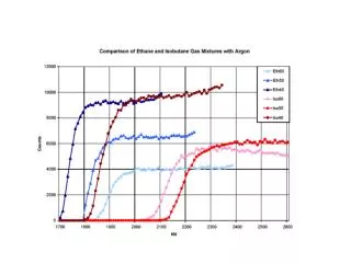
9/18 Ar Iso (95:5) B = 5T Resolution at 5T vs. gas mixtures • ~ 50 µm independent of the drift distance!! • σ ~ 1/40th of pad width!! (to compare √(12) ~=3.5) 50 mm
Concept Reality Making a versatile and valid technology.
10/18 Technical Hurtles. • Resist technology must be Micromegas Bulk Technology compatible, if it is to be used with Micromagas • Resistive layers must be able to withstand heat, chemical washing, mild friction… • Must be producible on large surface areas, preferably at low cost • Cost/unit area must be kept low (as always). • Charge evacuation rate from the surface of the resistive layer must be consistent with expected signal frequency to avoid signal pileup/gain fluctuations. • Further studies on both actual and desirable charge distributions are required to maximize and understand achievable resolution. • The effects on two track resolution must also be evaluated.
11/18 The Bulk technology
13/18 Pad Response Function (PRF) Question(s): Charge distribution questions. • What is the best PRF for a given pad pitch/layout? • What types of PRFs are possible; • Are multi-dimensional PRFs capable of achieving better resolution given the strong dependency on location of rise time for neighboring pads? • Is the complete parameterization of resistively distributed signals possible? • How is the charge distributed to the pads dependent on the resistive layer properties? • Can low resistivity films be used to channel signal conductively into the different pads, rather then inducing signal via capacitance coupling? • Would this be better in any way?
14/18 One Quick note on Multi dimensional PRF For resistive films electrically isolated from the readout pads, where a grounding guard ring is used to evacuate charge from the film, the total charge summed over central pad, plus the two pads to the left and right rises, then remains constant for a period of time. The signal decays off the central pad, and onto neighboring pads in turn, becoming shallower in amplitude and slower in rise time each consecutive pad till the charge is evacuated by the guard ring. The rate which it decays onto a neighboring pad is also dependent on where the charge was deposited on the principle pad. . . so by measuring the rise times of the central pad, and its neighbors one can also extract position information. This second dimension of information can be processed in parallel with amplitude information to yield a multi-dimensional PRF
15/18 A neat new idea?: Another possibility for pads, Thin.
16/18 How resistive are we talking? Methods and regimes • Films from CERN: stereography • 20 μm (~4000 ohm-cm, or ~16000 ohm-cm) (2 and 8 Mega Ohm / Square) • Bulk compatible (Saclay already has one and is testing it now) • Either with electrically insulating glue layer or without. • Films Via Carleton: Kapton film with sputtered distributed resistance on one side. • Similar process to COSMo TPC: It’s been done, and it works • Kapton film is press-glued onto readout board in a lamination process. • May be difficult to incorporate with bulk Technology, depending on thickness and robustness of sputtered layer • Films Via Neuchâtel: deposited amorphous silicon • Two deposited layers of amorphous silicon doped to varying degrees to control conductivity. • First possible regime: Carleton-esque 10^4 ohm cm layer sitting on a 10^11 ohm cm isolating layer. • Second possible: semi-conductive solution 10^-1 ohm cm layer sitting on a 10^4 ohm cm conductive layer, charge is split conductively as opposed to via capacitance coupling.
17/18 Possible Applications • ILC • T2K • S-LHC Atlas Upgrade • Compass • Timepix
17/18 Conclusions • Restive film technology is possible, and is being used to break resolution records with large pads. • We still have much to learn about resistive films and how to best use them; either to protect sensitive Timepix chips, or to protect large pad electronics and improve resolution of large pad systems.