Download
1 / 15
150 likes | 406 Views
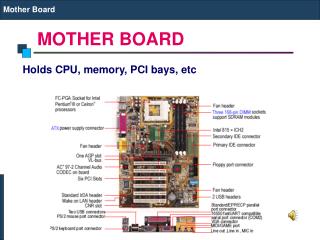
Elefant. Pre-amp. ADC. TDC. Pipe line. Memory. Event Buffer Memory. Pad Mother Board. Anode Mother Board. Memory. FPGA control. Serial Link to ROM. Sub-Trans. Board. PreAmp Comparisons. 2 nd Page. Front end prototype Board. VCC. ASD-4. ADC out. 16 variable shaping time

E N D
Elefant Pre-amp ADC TDC Pipe line Memory Event Buffer Memory Pad Mother Board Anode Mother Board Memory FPGA control Serial Link to ROM Sub-Trans. Board
Front end prototype Board VCC ASD-4 ADC out 16 variable shaping time Diff. Driver for ADC Input connector VCC TDC out
Function of this board • 16 channels LVDS output for TDC • 16 channel shaping amplifier (20-100ns integration time adjustable). 20ns for anode signal allowing higher rate. 100ns for pads signal for lower noise. • Differential output driver to ADC for reduce ground loop noise. • Flexible cable will be used and tested for signal attenuation, crosstalk, noise immunization and reflection. • Three layer of the prototype will be test to know the Z-resolution, tracking residual, and other properties.
2nd Prototype • Approximately Correct Geometry • 3 Layers – 2 Resistive + 1 Conductive • 50 cm Long • Purpose • Test Electronics • Comparison to Pspice model of 1st Prototype • Realistic Strip Geometry and Flex Cables • Pre-Amp Costs • KEK Chip – 550 yen/chip (4 channels) • 2000 Chip minimum order (Sony) • Require ~30k channels (with spares) – ($34k chips + $50k boards) • Elefant Chip • To Submit from US $8,680 – from Shanghai $3,400 • Production Cost for 10-12 wafers $200k • Designed in US (final design at LBL) Tested in China
Multi-Channel Timing & Amplitude Digitizer (MCTAD) front-end chip redesign Requirements ------------------------------------------------------------------------------- MCTAD is an acronym of an ASIC, which is designed for simultaneously digitizing the timing and waveform of a random signal, and store in a pipeline. The digital data will keep long enough (maximum 255 clock cycles) for the latency of the trigger condition is satisfied. The timing resolution is ~1/64 of the clock time, the amplitude readout will have 9 bit dynamic range with 7 bit log scale accuracy. The analog gain can be adjusted at the input stage by 4 time. The total record length of the amplitude can be 8 - 32 time slice. . The system clock can be adjusted from 20 –60 Mhz. This requirements are derived from "MECO tracker conceptual design", it also will suitable for many other applications. -------------------------
The FADC sampling clock can be selected to equal or one half of the system clock. That means the ranges of time slice from 16.6ns to 100ns, and record length from 130 ns to 3200 ns. The timing resolution will be 0.26 ns to 1.56 ns. The trigger latency buffer time will be 4.2 s to 25.5 s. The pedestal less than 20 mV with an full range of 2.0 volt. The peaking time is adjustable by the analog shaping stage of the preamplifier. The bandwidth of the analog input stage will be greater than 40 MHz. The digital input timing jitter will less than 200 ps.
A. DAQ Input Requirements: There will be at least 4 event storage buffers. Each channel will output a fast trigger data bit. B. Analog input stage requirements: The Analog Receiver is required to convert the 300mV-1.2V differential signal from the pre-amplifier IC to the 0.5 – 2.5v single ended drive to the FADC.
1. Signal Input Impedance Rin > 1megaOhms||Cin < 30pF 2. Signal Input Common Mode Voltage max < Vdd = 3.3V min > Vss = 0V 3. Output Frequency Response will be CR-RC. With Cload<5pF, Rload>100megaOhms 3dB lowpass < 100kHz -3dB hipass > 5megaHz 4. Peak Gain over Linear Range gain for 10ns step input min > 9.5 max < 10.5
5. Output Voltage Range for 1% Gain Linearity min < 0.5v max > 2.5v 6. Output Offset Voltage relative to Output Reference Voltage min > -40 mV max < 40mV7. Common Mode Rejection Ratio min > 60dB up to 10kHz8. Power Supply Rejection Ratio min > 60dB up to 10kHz9. Input Referred Noise over the pass band Vn < 50nV-rtHz In < 10pA-rtHz10. Gain adjustment 2 bits.11. Analog input signals per channel: Vdiff+ positive differential input voltage ( 1.2 –1.5 V)Vdiff- negative differential input voltage (1.2 – 0.9 V)
C. Digital Receiver requirements: The Digital Receiver is required to convert the LVDS differential signal from the Amplifier IC (assuming a 100 to 200 ohm impedance to Vdd) to the 0 – 1.8/2.5 V (core) single ended drive to the TDC. 1. Signal Input Impedance Rin > 1megaOhms Cin < 4pF 2. Signal Input Common Mode Voltage max < Vdd min > Vss + 1.5v 3. Propagation delay 10-90% with Cload<5pF, Rload> 100megaOhms min > 1ns max < 2ns 4. Propagation delay jitter max < 0.2ns
5. Common Mode Rejection Ratio min > 60dB up to 10kHz 6. Power Supply Rejection Ratio min > 60dB up to 10kHz 7. Signals per channel: Vdiff+ positive differential input voltage Vdiff- negative differential input voltage Vout positive single ended CMOS core voltage
D. Required Power voltage and Signals level:1. VDD +3.3V2. VSS ground3. VRef the output voltage reference1.250V4. Voh 1.350V5. Vol 1.150V6. Clock and control slew rate ( 5-20ns ) E. Possible Adjustments per chip:1. Vbrise adjust the rise time2. Vbfall adjust the fall time3. clock dividing 1bit4. gain adjusting 2bits