Download
1 / 7
70 likes | 300 Views
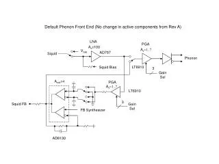
LNA DC Bias Module. Sander Weinreb, Jet Propulsion Laboratory, Caltech Glenn Jones, Jet Propulsion Laboratory, Caltech Requirements Approach Block Diagram Schematic Program Plan. Requirements.

E N D
LNA DC Bias Module Sander Weinreb, Jet Propulsion Laboratory, Caltech Glenn Jones, Jet Propulsion Laboratory, Caltech Requirements Approach Block Diagram Schematic Program Plan
Requirements • Provide 2 gate bias voltages and 2 drain bias voltages for four LNAs (2 X-band and 2 Ka-band) in the cryogenics dewar • All 16 outputs are adjustable with drains from 0 to 2.5V at up to 50ma and gates from -0.8 to +0.8V at 500uA. • All 16 outputs will have current monitoring, ground referenced and isolated by op amps. • Outputs shall be stable for capacitive load of 0.1 uF at end of 3' cable. • Internal voltage regulators so outputs are insensitive to supply voltages of +5 and -15V • No overvoltage on LNA for failure of a power supply voltage • Low cost manufacture
Approach Three approaches which have been used for LNA bias of many cryogenics amplifiers at JPL and NRAO: • Constant drain-current, feed-back control of gates • Constant gate voltage through gate voltage divider to protect HEMTs • Constant gate voltage with gate protection diodes in LNA Approach 3. has been selected because it allows gate current monitoring (a critical parameter for sensing transistor condition) and requires less wires that 1. Tests have shown that the stability of LNAs biased by any of these methods is similar.
Implementation Plan Present Status • Design complete, all parts on hand, and breadboard of drain circuit tested with capacitive load. For 3 x 6m Array Breadboard • Construct 3 modules for first 3 antennas; first by Jan 15, 2003 Further Development • Investigate digital pot version.