LNA progress
This document outlines the progress of LNA design and system testing, focusing on two PAD front-end concepts. We are concentrating primarily on differential designs while also developing a single-ended design. Key activities include characterizing devices at various operating temperatures (350K to 77K), addressing testing and test plan issues, and analyzing device cross-coupling effects. Current devices under evaluation include 70nm GaAs mHEMT and 100nm InP pHEMT technologies. We are committed to developing LNAs that integrate effectively with antennas, ensuring minimal noise implications.

LNA progress
E N D
Presentation Transcript
Current work overview • LNA designs to perform system tests of 2 PAD and validate 2PAD front-end concept • Concentrating on differential designs but have 1 single-ended design in fabrication • Characterising devices at various possible operating temperatures (including commercial devices) • Testing and test plan issues • Array cross-coupling
Device characterization • Measuring and characterizing devices in terms of small signal and noise parameters • Range of temperatures: 350K – 77K • On-wafer and packaged tests • Current devices under test: • 70nm GaAs mHEMT • 100nm InP pHEMT • 0.5um GaAs pHEMT E-mode • 0.5um GaAs HEMT D-mode
LNA Design I • Single-ended MMIC LNA using 70nm mHEMT process at OMMIC • Bandwidth 300 MHz – 3 GHz • Simulated noise temperature ~ 22K • Simulated gain ~ 35 dB • Delivery due October 2008
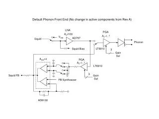
LNA Design II / III • Differential LNA – 2 designs • Using COTS components • FHC40LG and ATF35143 (lower noise resistance) (commercial GaAs HEMTs / pHEMT) • Input impedance designed for antennas developed by UoM and ASTRON • Prototype I measured at room temperature • Construction of prototype II underway – measurements scheduled for end of October 2008 Personnel responsible for LNA design MUST consider integration with antenna AND packaging issues
Array cross-coupling • Noise implications of antenna array cross-coupling • Investigating fundamental principles • Developing ADS model • Performing measurements on commercial packages LNAs
Conclusion • Transistor modeling and optimization (still) crucial! • Noise budget leaves not much room in 35K target • Closer cooperation and system noise tests required • And, Steve T, we indeed want to work in phase!