Download
1 / 1
10 likes | 125 Views
This project proposes a Silicon-on-Glass-based bulk-micromachined capacitive MEMS dual axis accelerometer design. The device senses acceleration along X and Y directions, enabling 2-axis inertial navigation applications. ANSYS simulation validates device functionality and sensitivity analysis. Optimized design parameters are derived for the accelerometer structure. MEMS accelerometers are vital in inertial navigation, airbag systems, etc. The novel design consists of an H-shaped movable mass supported by folded and straight beams for accurate acceleration detection. Stress analysis reveals regions for potential design improvement to enhance device reliability.

E N D
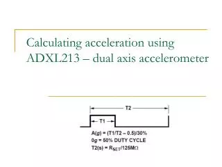
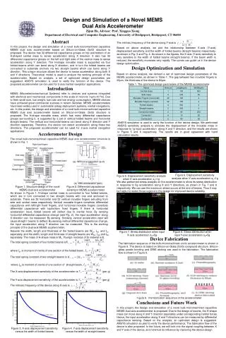
Design and Simulation of a Novel MEMS Dual Axis Accelerometer Zijun He, Advisor: Prof. Xingguo Xiong Department of Electrical and Computer Engineering, University of Bridgeport, Bridgeport, CT 06604 Abstract The intrinsic frequency of the device along Y-axis is In this project, the design and simulation of a novel bulk-micromachined capacitive MEMS dual axis accelerometer based on Silicon-on-Glass (SoG) structure is proposed. The device has 32 differential capacitance groups on top and bottom of an H-shaped central mass to sense acceleration along X direction. It also has 32 differential capacitance groups on the left and right side of the central mass to sense acceleration along Y direction. The H-shape movable mass is supported via four folded beams which can bend along X direction, and in turn the folded beams are connected to substrate anchors via two straight beams which can bend along Y direction. This unique structure allows the device to sense acceleration along both X and Y directions. Theoretical model is used to analyze the working principle of the accelerometer. Based on analysis, a set of optimized design parameters are suggested. ANSYS simulation is used to verify the function of the device. The proposed accelerometer can be used for 2-axis inertial navigation applications. Based on above analysis, we plot the relationship between X-axis (Y-axis) displacement sensitivity and the width of folded beams (straight beams) respectively, as shown in Fig. 3 and Fig. 4. As shown in the figures, the X-axis (Y-axis) sensitivity is very sensitive to the width of folded beams (straight beams). If the beam width is reduced, the sensitivity increases very rapidly. The curves can guide us in the device design optimization. Design Optimization and Simulation Based on above analysis, we derived a set of optimized design parameters of the MEMS accelerometer, as shown in Table 1. The gap between two movable fingers is 20μm, the thickness of the device is 80μm. Table 1. The optimized design parameters of the MEMS accelerometer Introduction MEMS (Microelectromechanical Systems) refer to devices and systems integrated with electrical and mechanical components in the scale of microns (1μm=10-6m). Due to their small size, low weight, low cost and low energy consumption, MEMS devices have achieved great commercial success in recent decades. MEMS accelerometers have been widely used in automobile airbag deployment systems, inertial navigations, etc. In this poster, the design and simulation of a novel bulk-micromachined capacitive MEMS dual axis accelerometer based on Silicon-on-Glass (SoG) structure is proposed. The H-shape movable mass, which has many differential capacitance groups surrounding it, is supported by a set of vertical folded beams and horizontal straight beams. The vertical and horizontal beams can bend along X direction and Y direction separately. Therefore, the device can detect acceleration along these two directions. The proposed accelerometer can be used for 2-axis inertial navigation applications. ANSYS simulation is used to verify the function of the device design. We performed ANSYS sensitivity analysis to simulate the displacement of the movable mass in response to 1g input acceleration along X and Y direction, and the results are shown in Figure 5 and 6 respectively. The results are in good agreement with hand calculation results. Accelerometer Design The novel bulk-micromachined capacitive MEMS dual axis accelerometer structure is shown in Fig. 1. (a). Without acceleration (a=0) Figure 7. Stress distribution when input X-axis acceleration ax=5g Figure 8. Stress distribution when input Y-axis acceleration ay=5g We also performed stress analysis on the accelerometer to show its stress distribution in response to 5g acceleration along X and Y directions, as shown in Fig. 7 and 8 respectively. We can see the maximum stress occurs at the end of beams. Thus it may be helpful to widen those regions in the design for improved device reliability. (b). With acceleration (a≠0) Figure 1. Structure design of the novel MEMS dual axis accelerometer Figure 2. Differential capacitance sensing in MEMS accelerometer As shown in Figure 1, H-shape central mass is connected to four folded beams, which are in turn connected to two straight beams with one end anchored to substrate. There are 32 horizontal and 32 vertical movable fingers extruding from side and central mass respectively. Vertical movable fingers constitute differential capacitance with left/right fixed fingers, and horizontal movable fingers constitute differential capacitance with top/bottom fixed fingers. If there is horizontal acceleration input, folded beams will deflect due to inertial force. By sensing horizontal differential capacitance change (see Fig. 2), the input acceleration along X direction can be measured. By sensing. Similarly, vertical acceleration input will cause straight beams to deflect. By sensing vertical differential capacitance change, the input acceleration along Y direction can be measured. This is the working principle of the dual-axis MEMS accelerometer. Figure 6. Displacement sensitivity analysis when Y-axis acceleration ay=1g Figure 5. Displacement sensitivity analysis when X-axis acceleration ax=1g Assume the width, length and thickness of the folded beams are Wb1, Lb1 and tb1 separately, and the width, length and thickness of straight beams are Wb2, Lb2 and tb2 separately. The mass of H-shape mass is Mh. Young’s modulus of Si material is E. Device Fabrication The total spring constant of four folded beams is The fabrication sequence of the bulk-micromachined comb accelerometer is shown in Figure 9. The device is based on Silicon-on-Glass (SoG) compound structure. Silicon-glass anodic bonding and DRIE etching are used in the fabrication. The fabrication flow is shown in Figure 9. where Ib1 is moment of inertia of one section of the folded beam, The total spring constant of two straight beams is where Ib2 is moment of inertia of one section of straight beam, Figure 3. X-axis displacement sensitivity versus the width of folded beams Figure 4. Y-axis displacement sensitivity versus the width of straight beams The X-axis displacement sensitivity of the accelerometer is (per g) The Y-axis displacement sensitivity of the accelerometer is (per g) The intrinsic frequency of the device along X-axis is Figure 9. The fabrication sequence of the accelerometer Conclusions and Future Work In this project, the design and simulation of a novel bulk-micromachined capacitive MEMS dual axis accelerometer is proposed. Due to the design of beams, the H-shape mass can move along X and Y direction separately under corresponding inertial forces. Hence, the input acceleration along X and Y directions can be measured by differential capacitance sensing. Based on the analysis, an optimized design is suggested. ANSYS simulation is used to verify the device performance. The fabrication flow of the device is also proposed. In the future, we will look into the signal coupling between X and Y axis of the device, and minimize its influence by improving the device design.